A universal asynchronous receiver/transmitter (UART).
Operation speed: 0-1.5M Baud (Baud is # of bits transmitted/sec, including start, stop, data and parity).
Includes:
A programmable Baud rate generator.
Separate FIFO buffers for input and and output data (16 bytes each).
Asychronous serial data:
Transmitted and received without a clock or timing signal.
Two 10-bit frames of asynchronous data.
7- or 8- bit ASCII, e.g. w or w/o parity, is possible.
Programmable Communications Interface: 16550
The 16550 can control a modem through DSR, DTR, CTS, RTS, RI and DCD.
In this context, the modem is called the data set while the 16550 is called the data terminal.
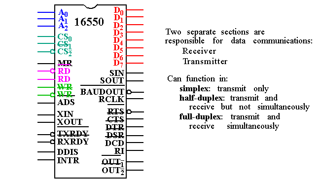
Pinout of the 16550
A0, A1 and A2: Select an internal register for programming and data transfer.
A2
A1
A0
Register
0
0
0
Receiver buffer (read) and transmitter holding (write)
0
0
1
Interrupt enable
0
1
0
Interrupt identification (read) and FIFO control (write)
0
1
1
Line control
1
0
0
Modem control
1
0
1
Line status
1
1
0
Modem status
1
1
1
Scratch
ADS: Address strobe used to latch address and chip select. Not needed on Intel systems -- connected to ground.
BAUDOUT: Clock signal from Baud rate generator in transmitter.
CS0, CS1, CS2: Chip selects
CTS: Clear to send -- indicates that the modem or data set is ready to exchange information. (Used in half-duplex to turn the line around).
Pinout of the 16550
D7-D0: The data bus pins are connected to the microprocessor data bus.
DCD: The data carrier detect -- used by the modem to signal the 16550 that a carrier is present.
DDIS: Disable driver output -- set to 0 to indicate that the microprocessor is reading data from the UART. Used to change direction of data flow through a buffer.
DSR: Data set ready is an input to 16550 -- indicates that the modem (data set) is ready to operate.
DTR: Data terminal ready is an output -- indicates that the data terminal (16550) is ready to function.
INTR: Interrupt request is an output to the micro -- used to request an interrupt.
Receiver error
Data received
Transmit buffer empty
Pinout of the 16550
MR: Master reset -- connect to system RESET
OUT1, OUT2: User defined output pins for modem or other device.
RCLK: Receiver clock -- clock input to the receiver section of the UART.
Always 16X the desired receiver Baud rate.
RD, RD: Read inputs (either can be used) -- cause data to be read from the register given by the address inputs.
RI: Ring indicator input -- set to 0 by modem to indicate telephone is ringing.
RTS: Request-to-send -- signal to modem, indicating UART wishes to send data.
SIN, SOUT: Serial data pins, in and out.
RXRDY: Receiver ready -- used to transfer received data via DMA techniques.
TXRDY: Transmitter ready -- used to transfer transmitter data via DMA.
WR, WR: Write (either can be used) -- connects to micro write signal to transfer commands and data to 16550.
XIN, XOUT: Main clock connections -- a crystal oscillator can be used.
Programming the 16550
Two phases: Initialization, operation.
Initialization:
After RESET, the line control register and baud rate generator need to be programmed.
Line control register sets the # of data bits, # of stop bits and the parity.
Addressed at location 011.
Stop bits: S = 1, 1.5 stop bits used for 5 data bits, 2 used for 6, 7 or 8.
Programming the 16550
Initialization (cont.)
ST, P and PE used to send even or odd parity, to send no parity or to send a 1 or a 0 in the parity bit position for all data.
ST
P
PE
Function
0
0
0
No parity
0
0
1
Odd parity
0
1
0
No parity
0
1
1
Even parity
1
0
0
Undefined
1
0
1
Send/receive 1
1
1
0
Undefined
1
1
1
Send/receive 0
No parity, both 0 -- used for internet connections.
SB = 1 causes a break to be transmitted on SOUT.
A break is at least two frame of 0 data.
DL = 1 enables programming of the baud rate divisor.
Programming the 16550
Initialization (cont.)
Baud rate generator is programmed with a divisor that sets baud rate of transmitter.
Baud rate generator is programmed at 000 and 001.
Port 000 used to hold least significant byte, 001 most significant.
Value used depends on external clock/crystal frequency.
For 18.432MHz crystal, 10,473 gives 110 band rate, 30 gives 38,400 baud.
Note, number programmed generates a clock 16X the desired Baud rate.
Last, the FIFO control register must be programmed at 010.
Programming the 16550
Operating:
Status line register gives information about error conditions and state of the transmitter and receiver.
This register needs to be tested in software routines designed to use the 16550 to transmit/receive data.
Suppose a program wants to send data out SOUT.
It needs to pool the TH bit to determine if transmitter is ready to receive data.
To receive information, the DR bit is tested.
Programming the 16550
Operating:
It is also a good idea to check for errors.
Parity error: Received data has wrong error -- transmission bit flip due to noise.
Framing error: Start and stop bits not in their proper places.
This usually results if the receiver is receiving data at the incorrect baud rate.
Overrun error: Data has overrun the internal receiver FIFO buffer.
Software is failing to read the data from the FIFO.
Break indicator bit: Software should check for this as well, i.e. two consecutive frames of 0s.
The other registers (for interrupt control and modem control) will be discussed in next chapter.
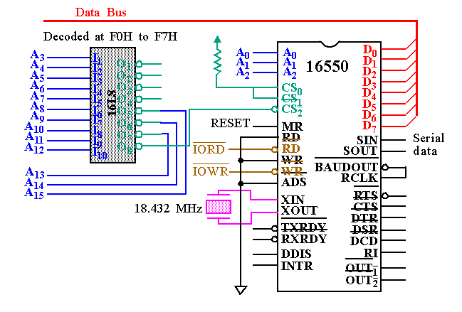
Example of 16550
Digital-to-Analog (DAC) Converters
Used to convert between analog and digital data.
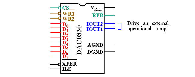
For example, the DAC 0830 (National Semi Corp.) is an 8-bit DAC that transforms an 8-bit binary number to an analog voltage.
8-bit yields 256 different analog voltages.
10-bit, 12-bit and 16-bit are also available.
Conversion time is 1us.
Digital-to-Analog (DAC) Converters
8-bit digital value drives D0 through D7.
The outputs are IOUT1 and IOUT2.
The output step voltage is defined by -VREF (reference voltage), divided by 255, e.g. if VREF = -5.0V, then the output step voltage is +0.0196.
The output step voltage is called the resolution of the converter.
Analog-to-Digital (ADC) Converters
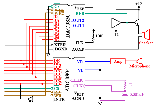
The ADC0804 is an 8-bit analog-to-digital converter that requires up to 100us to convert an analog input voltage into a digital output.
To start conversion, WR is pulsed with CS at GND.
The INTR pin signals the end of the conversion process.
Analog-to-Digital (ADC) Converters
VI- and VI+ are connected to an internal operational amplifier.
The ADC0804 requires a clock, generated either with: