Instructor:
-
Professor Jim Plusquellic
Text:
-
Computer Architecture: A Quantitative Approach,
-
by John L. Hennessy and David A. Patterson.
Supplementary texts:
-
Logic and Computer Design Fundamentals
-
by M. Morris Mano and Charles R. Kime.
Further Info:
-
http://www.cs.umbc.edu/~plusquel/611/index.html
-
To introduce many of the methods used by designers to implement general purpose processors and computer systems in general (CPU, I/O, memory and networks).
-
To introduce methods of analyzing CPU performance, in order to identify bottlenecks.
-
To expose you to various characteristics of today's architectures, i.e. Pentium/Merced, PowerPC, DEC Alpha, Sun SPARC, HP PA-RISC, MIPS, ...
-
Predominant technology: CMOS (Complimentary Metal Oxide Silicon)
-
Technology generation defined by:
-
Feature size: Size of the smallest features on an IC, usually the length of the transistor channel.
-
Current feature size: 250 nm.
-
What are the leading obstacles in reducing feature size ?
-
Photolithographic tools:
-
Current optical techniques: 248 nm wavelength can reduce feature size to 180 nm.
-
Next (and probably last) generation of optical lithography: 193 nm wavelength can reduce feature size to 130 nm, possibly down to 100 nm.
-
Contending solutions for 100 nm and below - see
Spectrum
, "Solid state", Jan. 1998).
-
Wires or interconnect: Currently aluminum
-
Problems:
-
-
Recently, IBM Corp. and Motorola Inc., Schaumburg, Ill. independently discovered way of replacing aluminum with copper.
-
-
Advantages:
-
Resistivity is 40 - 45% lower.
-
Reduced capacitance since smaller wires are possible, reduce cross-talk.
-
Reliability improved because of higher tolerance to electromigration.
-
No stress migration occurs.
-
Intel Chairman, 1965, Gordon Moore
-
Moore's Law:
-
# of transistors in IC will double every 18 months.
Offical Semiconductor Industry Association (SIA) Roadmap
|
|
1995
(350 nm)
|
1998
(250 nm)
|
2001
(180 nm)
|
2004
(130 nm)
|
2007
(100 nm)
|
2010
(80 nm)
|
|
DRAM (bits)
|
64M
|
256M
|
1G
|
4G
|
16G
|
64G
|
|
MPU transistors/cm
2
|
4M
|
7M
|
13M
|
25M
|
50M
|
90M
|
|
DRAM chip size (mm
2
)
|
190
|
280
|
420
|
640
|
960
|
1400
|
|
MPU chip size (mm
2
)
|
250
|
300
|
360
|
430
|
520
|
620
|
-
Accurate for last 20 years.
-
Will it hold for the next 15 years ? Will it fail due to physics or economics ?
-
Lithographic limits, design and test complexity and/or fabrication costs.
-
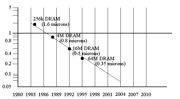
Moore's Law:
-
Minimum transistor feature size must decrease by a factor of 0.7 every three years:
-
Moore's Second Law:
-
The cost of building a semiconductor fab is doubling every three to four years.
-
In 1995, approximately 50 fabs in operation all over the world. Another 50 in some state of completion.
-
Current cost > $1 billion
-
Toshiba predicts cost of building mega-fabs may slowdown Moore's first law.
-
Companies joining forces: e.g. IBM/Siemens(64Mbit technology) and IBM/Siemens/Toshiba(256Mbit) joint developments.
-
Physical Limits:
-
Joel Birnbaum, HP senior president of R&D, EE times quote:
-
"In 2010, we will run into the physical limitation of having a fraction of an electron show up at a gate to switch the state of the transistor"
-
Pentium Pro:
-
Speed: 333 MHz
-
Number of transistors: 7.5 million
-
Supply voltage: 3.3 system, 2.8 processor
-
Technology: 250 nm
-
Speed: 300 MHz
-
Maximum current: 14.2 Amps
-
Power: 43 Watts
-
System bus speed: 66 MHz
-
Level 1 cache speed: 300 MHz
-
Level 2 cache speed: 150 MHz
-
Die size: 560 mils/side
-
PowerPC (604e):
-
Speed: 250 MHz
-
Number of transistors: 5.1 million
-
Supply voltage: 3.3 system, 1.9 processor
-
Technology: 250 nm
-
Power: 6 Watts
