by
Jeff Beasley
jbeasley@nmsu.edu
Department of Engineering Technology
New Mexico State university
and
William Hudson
hudson@ksu.edu
Department of Electrical and Computer Engineering
Kansas State University
Abstract: This paper presents a technique for creating CMOS combinational circuits using discrete MOSFET transistors. The material presented is suitable for use in an introductory circuits course. The nmos and pmos transistors are approximated as ideal switches. Included in this paper are examples of several CMOS logic circuits implemented at the transistor level along with a design method for the implementation of CMOS combinational logic circuits. Examples are also provided which show how the logic circuits can be simulated at the SPICE level incorporating typical fabrication model parameters. The paper concludes with a discussion on using the CD4007 CMOS transistor array package for implementing CMOS logic circuits.
Complementary Metal-Oxide Semiconductors (CMOS) logic devices are the most common devices used today in the high density, large number transistor count circuits found in everything from complex microprocessor integrated circuits to signal processing and communication circuits. The CMOS structure is popular because of its inherent lower power requirements, high operating clock speed, and ease of implementation at the transistor level. Students in introductory electronic circuits classes can gain insight into the operation of these CMOS devices through a few exercises in constructing simple CMOS combinational logic circuits such as AND, NAND gates, OR, NOR gates and INVERTERS. These circuits are created using both p and n-channel Metal-Oxide Semiconductor Field Effect Transistors (MOSFET) connected in complementary configurations.
The complementary p-channel and n-channel transistor networks are used to connect the output of the logic device to the either the VDD or VSS power supply rails for a given input logic state. In a simplified view, the MOSFET transistors can be treated as simple switches. This is adequate for an introduction to simple CMOS circuits where switching speeds, propagation delays, drive capability, and rise and fall times are of little concern.
Schematically MOSFET transistors are typically identified using three possible schematic symbols. These symbols are shown in Fig. 1 for both n-channel (nmos) and p-channel (pmos) devices.
The MOSFET schematic symbols shown in Fig. 1 (a) show the drain(D), gate(G), source(S), and bulk(B) connections for the transistor. The bulk, also called the bulk-substrate or substrate, is shown unconnected in this schematic symbol but must be properly connected before power is applied.
MOSFET Rule #1 - The bulk connections for MOSFET transistors are normally connected to a power supply rail. P-channel bulk connections are typically tied to the VDD rail and n-channel bulk connections are typically tied to the VSS rail.
The MOSFET schematic symbols shown in Fig. 1 (b) show the symbols for the p- and n-channel MOSFET transistors when the source-bulk connection has been shorted (VSB = 0.0 V). These symbols are most commonly used in documenting analog CMOS circuits.
The MOSFET schematic symbols shown in Fig. 1 (c) show the schematic symbols for p- and n-channel MOSFET transistors. In this case the bulk-substrate connection is not indicated. Notice too that the gates for the p- and n-channel devices differ. The p-channel device is identified by a "bubble" on the gate input. The n-channel device does not have a "bubble". The presence or absence of a "bubble" on the gate input is used to signify what logic level is used to turn-on the transistor. The presence of a "bubble" on the p-channel device indicates that this device should have a logic low applied to the gate input to turn-on the transistor while the absence of a "bubble" on the n-channel device indicates that this device should have a logic high applied to the input to turn-on the device. These schematic symbols are most commonly used when documenting CMOS logic circuits. The bulk-substrate connections are almost always connected to the power supply rails using MOSFET Rule #1.
The MOSFET transistor has three major regions (modes) of operation: cutoff, saturation and non-saturated region. In the non-saturated (or triode) region, the voltage drop across the drain-source terminals approaches zero volts as the magnitude of the voltage drop across the gate-source terminals approaches VDD - VSS. For example, in a 5 volt system, the drain-source voltage approaches zero volts as the magnitude of the gate-source voltage drop approaches 5 volts. In the cutoff region, the drain-to-source current, IDS, approaches zero amps (i.e. the drain-source resistance approaches infinity - an open circuit). Hence, the drain and source terminals of a MOSFET transistor can be treated as an ideal switch alternating between the off (cutoff) and on (non-saturated) modes of operation. However, there is a limitation on the use of the MOSFET transistors as ideal switches:
MOSFET Rule #2 - For proper operation as an ideal switch, the p-channel MOSFET transistor or network must be connected to the most positive voltage rail while the n-channel MOSFET transistor or network must be connected to the most negative voltage rail.
III. The AND/OR and Inverter Structure
Creating "AND" and "OR" structures using MOSFET transistors is easily accomplished by placing the nmos and pmos transistors either in series (AND) or parallel (OR) as shown in Fig. 2 and 3. Shown in Fig. 2 (a) and (b) are two MOSFET transistors connected in series. The singular current path in both structures defines the "AND" operation. Shown in Fig. 3 (a) and (b) are two MOSFET transistors connected in parallel. The parallel current paths represent the "OR" structure.
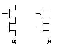
Fig. 2 (a) nmos "AND" structure
(b) pmos "AND" structure
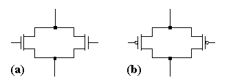
Fig. 3 (a) nmos "OR" structure (b) pmos "OR" structure
Figure 4 shows an nmos "AND" structure
with the source of M1 connected to ground (MOSFET Rule #2). An nmos switch
is turned-on when a logic high is applied to the gate input. The logic expression for the circuit
shown in Fig. 4 is 
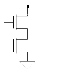
Fig. 4 An nmos Transistor Structure Realizing the expression F = (A B)-L
Creating a CMOS inverter requires only one pmos and one nmos transistor. The nmos transistor provides the switch connection to ground when the input is a logic high while the pmos device provides the connection to the VDD power supply rail when the input to the inverter circuit is a logic low. This is consistent with MOSFET Rule #2. The transistor configuration for a CMOS inverter is shown in Fig. 5.
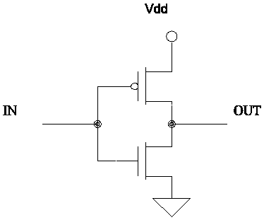
Fig. 5 The transistor view of a CMOS Inverter
IV. A Design Procedure for Creating CMOS Combinational Logic Circuits
The following design process [1] provides a method for obtaining an optimal CMOS combinational transistor structure given a functional (Boolean) expression. The method is based on the use of mixed logic concepts. The input variables should have a designated assertion level (i.e. Assert Low or Assert High).
In CMOS designs, two transistor structures (one pmos and one nmos) are required for implementing the functional expression. In logic systems, the analogous expression defines what is required to generate the required output assertion level. The complementary expression, obtained by applying DeMorgan's theorem to the functional expression, defines the complementary structure. These two expressions, the analogous and the complementary, are then used to create the transistor network for a CMOS circuit. The design procedure is described as follows in five steps.
1. Identify the "most common" input level by examination of the input assertion levels. This requires that the input assertion levels be defined. An input variable containing a conflict is treated as if it has the opposite assertion level. The "most common" input level will be either "Low" or "High". This is determined by counting the number of asserted high or asserted low inputs after adjusting for conflicted inputs.
2. The "most common" input level is used to specify the type of transistors used for implementing the analogous structure
| Most Common Input Level | Analogous Structure |
|---|---|
| LOW | PMOS transistors are used to create the analogous structure |
| HIGH | NMOS transistors are used to create the analogous structure |
3. If there is not a "most common" input level then select the input level to be the opposite level of the required output assertion level.
4.(a) Create the analogous transistor structure directly from the functional logic expression. Use the transistor type specified in part 2 for creating the structure.
4.(b)The complementary structure is created by applying DeMorgan's theorem to the analogous expression. The transistor type is opposite to that used in part 4(a).
5. Assemble the analogous and complementary structures to create the full CMOS equivalent circuit. In some cases, an inverter must be added to the output of the circuit to correct the output assertion level.
Example 1:
Given 

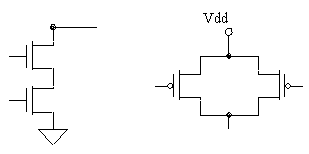
Fig. 6 The (a) analogous and (b)
complementary structures for Example 1
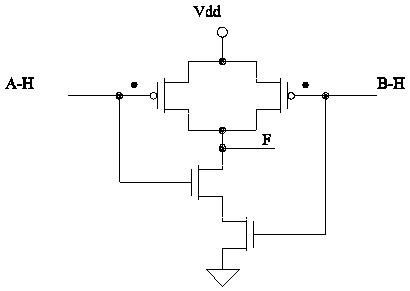
Fig. 7 The Complete Transistor Circuit
for Realizing the Expression 
Example 2:
Given: 

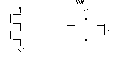
Fig. 8 The (a) analogous and (b) complementary structures for Example 2
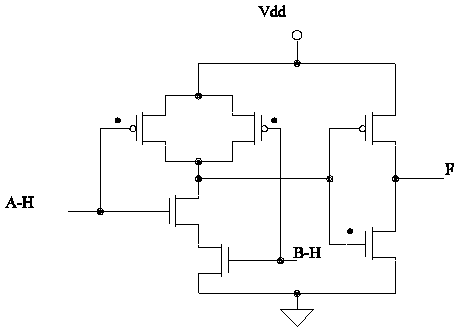
Fig. 9 The Complete Transistor Circuit
for Realizing the Expression 
The procedures and results for creating the transistor equivalent circuits in Example 1 and Example 2 are the same except that the circuit in Example 2 required the placement of an inverter on the output to correct the assertion level to match desaign specifications. The logic circuit created in Example 1 is commonly called a Positive Logic NAND gate. The logic circuit created in Example 2 is commonly called a Positive Logic AND gate. This procedure can be easily applied to create NOR, OR, XOR, XNOR gates
Example 3:

Given:


Fig. 10 (a) the Analogous and (b) Complementary Structure
Fig. 11 The Complete Transistor Circuit
for Realizing the Expression 
V. SPICE simulation of a CMOS logic circuit
The CMOS logic circuits described in part IV can be simulated using SPICE. Accurate transient response (rise/fall time, propagation delay, etc.) of the circuit can be modeled by incorporating proper fabrication model parameters. MOSIS [3] fabrication parameters have been used in the simulation. It is important to observe that the SPICE simulation is an analog simulation. One can observe the behavior of the transistor networks throughout the entire transition. While this gives an accurate picture of the circuit's analog behavior it is not very fast or practical for large transistor count circuits.
Two SPICE simulations will be discussed in this section. For help with any of the SPICE commands refer to SPICE: A Guide to Circuit Simulation and Analysis Using PSPICE by Tuinenga [4]. The first SPICE simulation will be for a CMOS inverter. The second SPICE simulation will demonstrate the operation of the "NAND" circuit created in Example 1 in part IV. A piece-wise linear approximation is used to model a ramp to the input to the CMOS inverter using the SPICE PWL option. This allows easy observation of the switching points of the device (Fig. 12) and allows observation of the transient current behavior as shown in Fig. 13
A SPICE Simulation of a CMOS Inverter.
 * A CMOS Inverter Using 2 Micron Channel Lengths
*
*   D G S B
MP1 5 1 3 3 CMOSP W=28.0U L=2.0U AS=252P AD=252P
MN1 5 1 0 0 CMOSN W=10.0U L=2.0U AS=90P AD=90P
VIN 1 0 PWL(0 0 100n 5.0 200n 0)
VDD 3 0 DC 5.0
*
*The following are fabrication parameters obtained
*from the MOSIS service.
.MODEL CMOSN NMOS LEVEL=2 LD=0.121440U TOX=410.000E-10
+ NSUB=2.355991E+16 VTO=0.7 KP=8.165352E-05 GAMMA=1.05002
+ PHI=0.6  UO=969.492 UEXP=0.308914 UCRIT=40000
+ DELTA=0.262772 VMAX=71977.5 XJ=0.300000U LAMBDA=3.937849E-02
+ NFS=1.000000E+12 NEFF=1.001 NSS=0 TPG=1.000000
+ RSH=33.290002 CGDO=1.022762E-10 CGSO=1.022762E-10
+ CGBO=5.053170E-11 CJ=1.368000E-04
+ MJ=0.492500 CJSW=5.222000E-10 MJSW=0.235800 PB=0.490000
* Weff = Wdrawn - Delta_W
* The suggested Delta_W is 0.06 um
*
.MODEL CMOSP PMOS LEVEL=2 LD=0.180003U TOX=410.000E-10
+ NSUB=1.000000E+16 VTO=-0.821429 KP=2.83164E-05 GAMMA=0.684084
+ PHI=0.6 UO=336.208 UEXP=0.351755 UCRIT=30000
+ DELTA=1.000000E-06 VMAX=94306.1 XJ=0.300000U
+ LAMBDA=4.861781E-02
+ NFS=2.248211E+12 NEFF=1.001 NSS=1.000000E+12 TPG=-1.000000
+ RSH=119.500003 CGDO=1.515977E-10 CGSO=1.515977E-10
+ CGBO=2.273927E-10 CJ=2.517000E-04  MJ=0.528100
+ CJSW=3.378000E-10
+ MJSW=0.246600 PB=0.480000
* Weff = Wdrawn - Delta_W
* The suggested Delta_W is 0.27 um
* .PLOT TRAN V(3) V(2) V(1)
.TRAN .1n 250n
.PROBE
.END
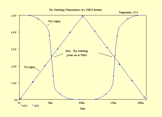
Fig. 12 . The SPICE Simulation
of the Switching Behavior of a CMOS Inverter.
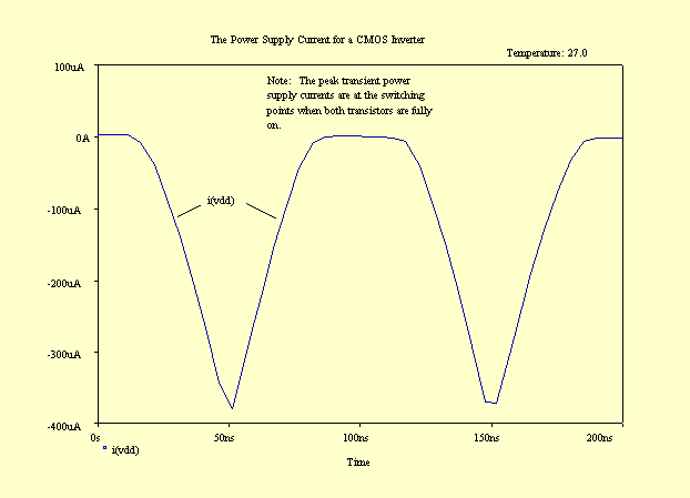
Fig. 13. The SPICE Simulation of the Transient Current Behavior of the CMOS Inverter.
A SPICE Simulation of a CMOS NAND Gate:
* A CMOS NAND gate Using 2 Micron Channel Lengths
*
*   D G S B
MP1 4 1 3 3 CMOSP W=28.0U L=2.0U AS=252P AD=252P
MP2 4 2 3 3 CMOSP W=28.0U L=2.0U AS=252P AD=252P
MN1 4 1 5 0 CMOSN W=10.0U L=2.0U AS=90P AD=90P
MN2 5 2 0 0 CMOSN W=10.0U L=2.0U AS=90P AD=90P
VINA 2 0 PULSE(0 5 100ns 5ns 5ns 100n 200ns)
VINB 1 0 PULSE(0 5 205ns 5ns 5ns 200n 400ns)
.TRAN .1n .5u
VDD 3 0 DC 5.0
*
*
.MODEL CMOSN NMOS LEVEL=2 LD=0.121440U TOX=410.000E-10
+ NSUB=2.355991E+16 VTO=0.7 KP=8.165352E-05 GAMMA=1.05002
+ PHI=0.6  UO=969.492 UEXP=0.308914 UCRIT=40000
+ DELTA=0.262772 VMAX=71977.5 XJ=0.300000U LAMBDA=3.937849E-02
+ NFS=1.000000E+12 NEFF=1.001 NSS=0 TPG=1.000000
+ RSH=33.290002 CGDO=1.022762E-10 CGSO=1.022762E-10
+ CGBO=5.053170E-11 CJ=1.368000E-04
+ MJ=0.492500 CJSW=5.222000E-10 MJSW=0.235800 PB=0.490000
* Weff = Wdrawn - Delta_W
* The suggested Delta_W is 0.06 um
*
.MODEL CMOSP PMOS LEVEL=2 LD=0.180003U TOX=410.000E-10
+ NSUB=1.000000E+16 VTO=-0.821429 KP=2.83164E-05 GAMMA=0.684084
+ PHI=0.6 UO=336.208 UEXP=0.351755 UCRIT=30000
+ DELTA=1.000000E-06 VMAX=94306.1 XJ=0.300000U
+ LAMBDA=4.861781E-02
+ NFS=2.248211E+12 NEFF=1.001 NSS=1.000000E+12 TPG=-1.000000
+ RSH=119.500003 CGDO=1.515977E-10 CGSO=1.515977E-10
+ CGBO=2.273927E-10 CJ=2.517000E-04  MJ=0.528100
+ CJSW=3.378000E-10
+ MJSW=0.246600 PB=0.480000
* Weff = Wdrawn - Delta_W
* The suggested Delta_W is 0.27 um
* .PLOT TRAN V(3) V(2) V(1)
.PROBE
.END
Fig. 14 The SPICE Simulation of a CMOS AND Gate.
VI. Constructing a CMOS logic circuit using the CD4007 transistor array package.
Once the logic circuit is designed and verified with SPICE, a CMOS hardware circuit can be created using the CD4007 CMOS transistor array package. The CD4007 contains six transistors, three pmos and three nmos transistors, which includes an inverter pair. The transistors are accessible via the 14-pin DIP terminals. A connection diagram and a schematic of the package are provided in Fig. 15. Proper bulk-substrate connections are already made in the device package.
Fig. 15 The CD4007 Transistor Array Package
A NAND gate (see Fig. 7) can be created using the CD4007 transistor array package by making the connections as shown in Fig. 16. The required connections are shown in red. Notice that there are common gate connections for pmos and nmos devices on Input A, pin 6 and Input B, pin 3. This is a convenient option for creating CMOS Combinational Logic circuits. The output is common to pins 1,5,13.
Fig. 16 An Implementation of a CMOS NAND gate Using the CD4007.
VII. Conclusion
This paper has presented a technique for creating CMOS logic circuits using discrete MOSFET transistors. The design technique provides a systematic method for designing and constructing any reasonably sized CMOS combinational circuit device. The technique assumes that MOSFET devices operate as ideal switches with only an "on" and "off" mode. For simple circuits, the omission of the switching transient behavior is acceptable as long as information regarding the operating speed and propagation delay and drive capability are not needed.
References
[1] W. Hudson, J. Beasley, and E. Steelman, "A CMOS Combinational Circuit-Design Method Using Mixed Logic Concepts," IEEE Transactions on Education, Vol. 38, No. 3, August, 1995, pps. 266-273.
[2] W. Hudson and J. Beasley, "The Mixed Logic Approach to Digital Design and Analysis" The Technology Interface, Vol. 1 No. 1, Fall 1996, http://et.nmsu.edu/~etti/fall96
[3] MOSIS, the Metal Oxide Semiconductor Implementation Service, USC Information Sciences Institute, http://www.mosis.org/
[4] P. Tuinenga, "SPICE: A Guide to Circuit Simulation and Analysis Using PSPICE 3rd edition," Prentice Hall, 1995