1) a) (15pts) Identify (give the name for) the structure given by the layout below. Label the nodes and briefly explain how it works.
b) (5 pts) What is the relationship between the 4 (left-most) transistors shown in the figure and the transistors (not shown) driving the M1 lines on the far right? (Hint: What must hold true in order for this circuit to work? Think beta)
2a) (5 pts) Vt is an important device parameter that must be precisely controlled by process engineers. What is the effect of lowering Vt in terms of propagation delay? Why must Vt be non-zero in CMOS?
b) (6 pts) Beta is another important parameter that effects Ids. What parameter(s) of beta do you have control over as a designer? What parameter(s) of beta are controlled by process engineers? What parameter(s) are controlled by the physical laws of the materials?
c) (5 pts) If  , what value of W do you need in order to make
  if the p-type doping density results in a hole mobility of
  ? Assume gate oxide thickness is uniform for both types of devices at
  and L = 1.
d) (4 pts) Briefly explain why it is not important to make  in self-loaded circuits. (Your answer should include references to drain and gate capacitance).
3)a) (12 pts) Label each transistor with its region of operation (assume Vt is 1 volt).
c) (8 pts) Compute the low and high noise margins using the following transfer curve of a Pseudo-pMOS inverter.

4)a) (4 pts) Given the following VHDL code:
a) (10pts) Give the truth table for the input-output functionality of the entity-architecture relationship of logicgate.logicgate_str.
b) (10 pts) Give the truth table for the input-output functionality of the entity-architecture relationship of main.main_str.
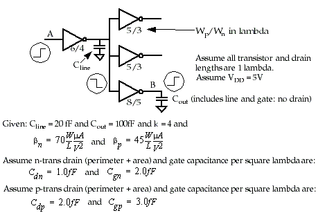
5) a) (6 pts) Name the three components of CL at the output of a gate.
b) (14 pts) Estimate the delay between nodes A and B for a rising transition on A using the simple gate delay model. CLEARLY INDICATE WHAT YOU ARE CALCULATING !!!!