-
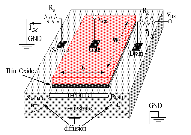
Metal gate has been replaced by polysilicon or poly in today's processes.
-
Can be used as a further mask to allow precise dfinition of the source and drain regions.
-
Minimizes gate-to-source/drain overlap which is good for performance.
-
MOS structure created by superimposing several layers of conducting, insulating and transistor-forming materials.
-
Construction process is carried out on a SINGLE crystal of silicon.
-
Wafers are 15-20 cm in diameter (6-8 inches).
-
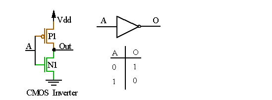
CMOS: Two types of transistors are used, pMOS and nMOS.
-
nMOS: negatively doped silicon, rich in electrons.
-
pMOS: positively doped silicon, rich in holes (the DUAL of electrons).
-
We can treat MOS transistors as simple on-off switches with a source (S), gate (G) (controls the state of the switch) and drain (D).
-
Let `1' represent high voltage, 1.5V to 15V (<= 3.3V today) (V
DD
).
-
Let `0' represent low voltage - GND or V
SS
.
-
Signals such as `1' and `0' have
strength
, measures their ability to:
-
Sink (to lower voltage, e.g. GND) or
-
Source (from higher voltage, e.g. V
DD
) current.
-
nMOS and pMOS signal transmission strength:
-
The reason p-transistors are poor transmitters of logic 0 and n-transistors are poor transmitters of logic 1 is related to threshold voltage (V
t
~= 700mV).
-
Threshold voltage is defined and discussed in detail in Chapter 2.
-
Under the "switch" abstraction, G has complete control and S and D have no effect.
-
In reality, the gate can turn the switch on only if a potential difference of at least V
t
exists between the G and S.
-
This is clearly not the case for the "weak" bias configurations and "weak" 0s (~700mV) and "weak" 1s (~4.3V) result.
-
The following (buffer) implementation is a BAD IDEA. Why?
-
The off state of a transistor creates a high impedance condition Z at the drain. No current flows from source to drain:
-
Complementary Switch or Transmission gate or Pass Gate:
-
This configuration allows `1's and `0's to be passed in an acceptable fashion.
-
When A = `0',
Out
is in a high impedance state (not driven by
In
).
-
If the gates of transistors P1 and N1 are not connected, then 4 possible output states are possible. What are the two additional states ?
-
Are any of these states undesirable ? Why ?
-
How would you implement this function using logic gates instead of CMOS switches ?
-
Master-Slave D Flip-Flop:
-
We will look at memory elements in much more detail later.
-
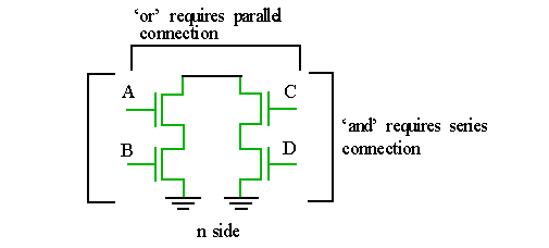
For the n-side, take the uninverted expression (the complement of F; F):
-
`and' expressions are implemented using series connections of n transistors.
-
`or' expressions are implemented using parallel connections of n transistors.
-
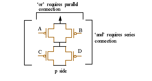
For the p-side, invert expression used for n-expansion:
-
`and' expressions are implemented using series connections of p transistors.
-
`or' expressions are implemented using parallel connections of p transistors.
-
Combine to build function:
Try building
-
You must master all of the following transformations between levels of abstractions:
-
1) The previous analysis shows how to take a Boolean expression and create a transistor-level schematic diagram.
-
However, it assumes the Boolean expression is already in the appropriate form, which may not always be the case.
-
Boolean expression reduction:
-
You should already know how to manipulate boolean expressions, e.g., using De Morgan's Laws, from exercises in other courses.
-
The objective is to reduce a boolean expression so that it can be realized in full-complementary CMOS using the minimum number of transistors.
-
In general, I am
not
expecting you to realize CMOS gates using
pass structures
in which the inputs are used to drive the output of the gate.
-
The XOR/XNOR implementations we saw earlier are examples of this.
-
The following heuristics can be applied as target reductions that will help you to obtain minimum realizations:
-
Since CMOS is naturally inverting, you'll want to target a final expression of the form:
-
Many times only
un
complemented literals are available as signals in your circuit. Therefore, the reductions should attempt to
remove
the complemented literals in the Boolean expression.
-
Application of De Morgan's Laws can be used to transform complemented literals to NANDs and NORs.
-
You should analyze each transformation to learn the trade-offs.
-
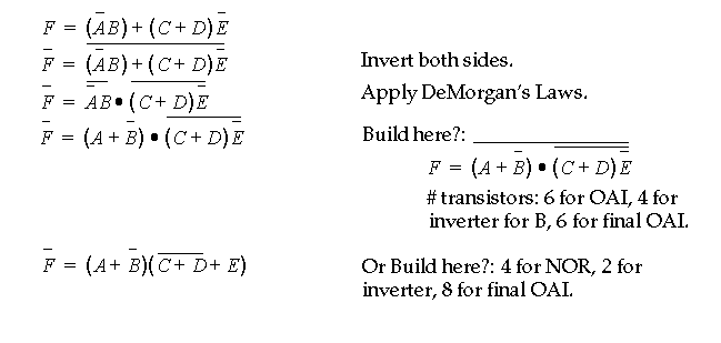
The following reduction sequence can be applied that targets NANDs and removes the complemented literals:
-
Note that further reductions to NANDs and NORs may not pay off in the previous case.
-
In the next case, it is possible to get rid of an uncomplemented literal without increasing the size of the OAI:
-
Further transformations are not useful -- convince yourself.
-
Expressions with repeated variables may be simplified to save a couple transistors:
-
Sometimes it is best to implement the
inverse
function and add an inverter.
-
For example, Carry, which has all uncomplemented inputs.
-
The best way to learn this is through practice.
-
Simply make up an expression of multiple variables and invert a couple of the literals and/or subexpressions.
-
2) Translating from
transistor-level schematics
to
Boolean expressions
is straightforward.
-
Simply write the
n-tree
expression using the rules for series and parallel transistors given earlier.
-
Invert the final expression.
-
3) Translating from
transistor-level schematic
diagrams to
layout
is covered in the laboratories.
-
4) Translating from
layout
to
transistor-level schematic
diagrams is also covered in the laboratories.
-
In general, start by identifying the transistor sources connected to V
DD
or GND nodes.
-
Add series transistors in the schematic for transistors whose sources are connected to drains of the previously identified transistors.
-
Add parallel transistors at fan-out points.
-
Label the transistors so it possible to connect the gates properly by tracing the poly connections.
