-
Need simple models to estimate system performance in terms of signal delay and power dissipation.
-
Issues include:
-
Resistance, capacitance and inductance calculations.
-
Delay estimations.
-
Determination of conductor size for power and clock distribution.
-
Power consumption.
-
Charge sharing mechanisms.
-
Design Margining.
-
Reliability.
-
Effects of scaling.
-
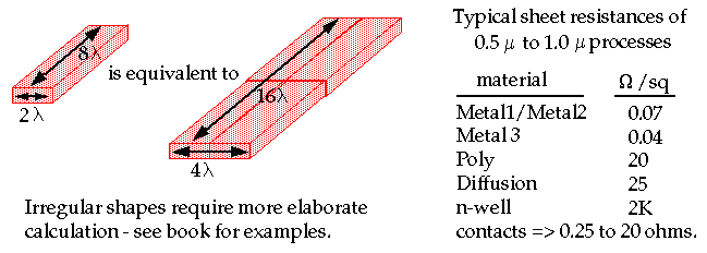
The resistance of a uniform slab of conducting material may be expressed as
-
For example, in a layout editor, such as magic or virtuoso:
-
Channel resistance can be estimated in the
linear
region as:
-
A range of 1,000 to 30,000 ohms/square are possible for n-channel and p-channel devices.
-
Typical betas for identically sized devices; n-dev: ~90, p-dev: ~30 microA/V
2
.
-
Temperature changes both mu (mobility) and V
t
(threshold voltage) and, therefore channel resistance.
-
Channel resistance increases with temperature, approximately +0.25% per degree C above 25 degrees.
-
Metal and poly resistance change about 0.3% and well diffusions about 1% per degree C.
-
Switching speed of MOS systems
strongly
dependent:
-
Parasitic capacitances associated with the MOS transistor.
-
Interconnect capacitance of "wires".
-
Resistance of transistors and wires.
-
Total
load
capacitance on the output of a CMOS gate is sum of:
-
Gate capacitance (of
receiver
logic gates downstream).
-
Driver
diffusion (source/drain) capacitance.
-
Routing (
line
) capacitance of substrate and other wires.
-
Let's consider approximations of each of these capacitances and subsequent approximations of delay based on these expressions.
-
The capacitance of a MOS transistor can be modeled using 5 capacitors.
-
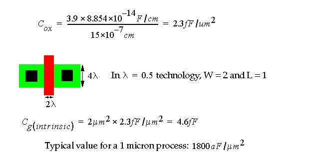
An approximation of gate capacitance (C
gs
, C
gd
and C
gb
) is given as:
-
For example, for thin-oxide thickness of 15 nm,
-
This is a conservative estimate of gate capacitance that does not include fringing fields (extrinsic) gate capacitance.
-
Gate capacitance increases as the thin-oxide thins.
-
An approximation (
lumped model
) of source/drain capacitance (C
sb
and C
db
) is given as:
-
This model assumes a zero DC bias across the junction.
-
Because of fan-out,
gate
capacitance usually dominates the loading.
-
Routing capacitance between metal and poly can be approximated using a parallel-plate model.
-
The effect of the fringing fields is to increase the effective area of the plates.
-
Appropriate if the wire delay is MUCH less than the gate delay, e.g.,
-
This expression derives from the expression for RC delay (we'll see this later).
-
As an example, assuming gate delay is 200ps, what is the maximum length of a minimal-width metal wire (in 1.0um technology) that we can use without worrying about the RC delay of the wire itself?
-
Assume Metal1 = 0.05 Ohms/square and 30 aF/um
2
.
-
But this assumes there is no gate load capacitance.
-
A conservative estimate is 5000 lambda (~16,330/3).
-
In a 1.0um process, RC delay MUST be considered for any wire > 2.5mm.
-
But for now, let's consider "electrical nodes" for which we can ignore distributed RC effects.
-
Our model and definitions:
-
Fall/rise time, e.g. t
f
, computed between 10% and 90% of V
DD.
-
Propagation delay, t
dr
, computed at 50% points on input and output waveforms.
-
How do we model gate delay?
-
Assume input is driven by a step waveform (unlike previous slide).
-
Approximation for fall time:
-
Note that the input waveform's finite slope will also effect this result -- adding a small amount of additional delay which is ignored here -- see text for details.
-
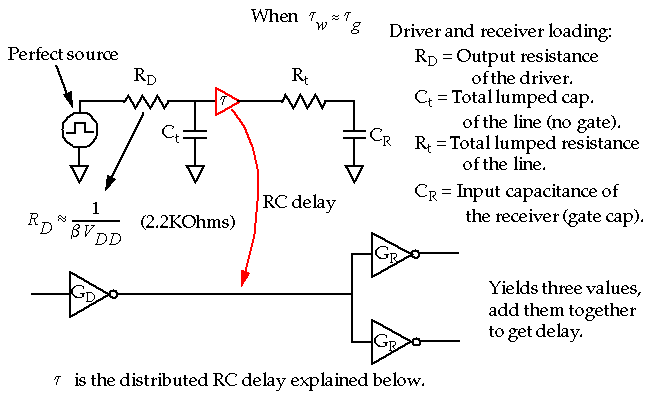
For example, let's compute the delay between G
D
and G
R
:
-
If the wire delay ~= gate delay, then we will have to use a different approximation consisting of three components:
-
A wire can be represented in terms of several RC sections:
-
A discrete analysis of this circuit yields an approximate delay of:
-
As n becomes large (and the sections becomes small), this reduces to:
-
RC effect dominates for very long wires due to l
2
term, e.g., doubling the length of the wire, quadruples the delay.
-
For example, consider a long poly wire:
-
The buffer is one possible method of reducing the propagation delay.
-
Assume r = 20 Ohms/micron and c = 0.4 fF/micron, then:
-
The buffer version is faster if its delay is less then 8ns. This is easily achieved.
-
When are distributed RC effects important to consider:
-
Long wires with high resistance, e.g. poly wires.
-
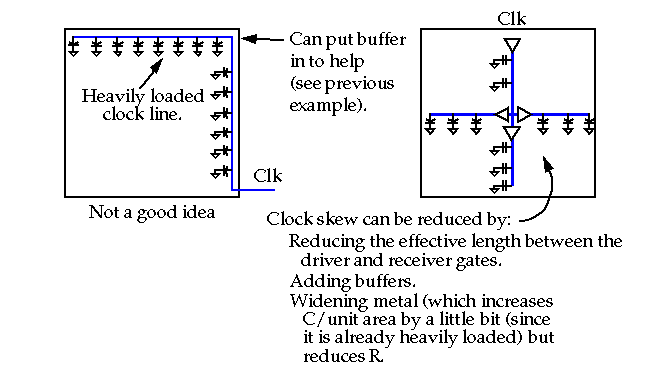
Long, heavily loaded clock lines.
-
An example showing that reducing R at the expense of C helps a lot in some cases:
-
Assume clock wire runs over 20mm and 50pF is distributed evenly along the line.
-
Assume r = 0.05 Ohms/um.
-
Then clock skew (delay to the end of the wire) is:
-
Solutions include adding a buffer, distributing the clock from the top center and/or widening the metal wire.
-
For example, reducing l to 10mm and widening the clock wire to 20um:
-
How does the distributed RC model differ from lumped model?
-
Note that these effects are completely ignored in the simple gate delay model.
-
FYI: We estimate delay using RC time constants assuming that the time taken for a signal to reach 62.3% of its final value approximates the switching point of an inverter.
-
Construct an equivalent inverter, e.g.,
-
3-input NANDs are closely balanced since n beta is about 3 times larger than p beta.


