-
So far we have looked at full complementary logic structures and the ratioed CMOS inverter.
-
Alternative CMOS logic configurations are also possible when designs are constrained by:
-
High-speed requirements
-
Low-power dissipation
-
Area or density
-
Full-complementary CMOS
will always
function correctly even in the presence of
noise
and with
low power-supply voltages
. "Safeness" of function.
-
In contrast, alternative CMOS logic configurations can produce incorrect functional behavior as a result of:
-
Insufficient power supplies or power supply noise.
-
Noise on gate inputs.
-
Incorrect ratios in ratioed logic.
-
Charge sharing or incorrect clocking in dynamic gates.
-
Both
functional
and
temporal
(timing) constraints must be met to ensure correct operation of an integrated logic gate.
-
When optimizing for speed, there are many more options from which to choose.
-
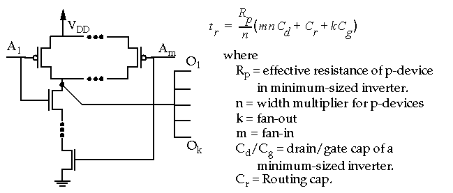
Our previous analysis determined that rise/fall time could be approximated by:
-
The number and size of transistors in series (or parallel) in the pull-down or pull-up path affects
 .
.
-
C
L
is affected by the size of the transistors in the gate (self-loading), the routing capacitance and the number and size of the driven transistors.
-
Note this approximation does not consider rise/fall time of the input signal.
-
In many designs, many logic paths do not require any special consideration.
-
Critical paths
: Paths that require attention to the timing details.
-
Automated design tools such as timing analyzers can automatically identify the slowest paths.
-
Timing analysis can be performed at the:
-
Architecture level.
-
RTL/logic gate level.
-
Circuit level.
-
Layout level.
-
Timing optimization has greatest impact if performed at the
architecture
level. This requires knowledge of:
-
How many gate delays fit into a clock cycle.
-
How fast addition occurs.
-
How fast memories access.
-
Timing optimization can also be performed at the
RTL/logic
level where design is focused on:
-
Pipelining.
-
The types of gates (INVERTER, NAND/AND, Complex gates, PLAs, etc.)
-
The fan-in and fan-out of the gates.
-
Circuit level optimization:
-
Sizing transistors.
-
Using alternative forms of CMOS logic.
-
Layout level optimization:
-
Critical paths are routed first to keep their interconnect distance small.
-
Loading capacitance and interconnect resistance considered more extensively, e.g., drain merging, choice of routing layer, etc.
-
Fan-in: The number of inputs on a gate.
-
Fan-out: Total number of gate inputs driven by a gate output.
-
Note: This value is usually expressed in some default gate size such as the number of minimum sized inverter gates.
-
How does fan-in affect the speed of the gate?
-
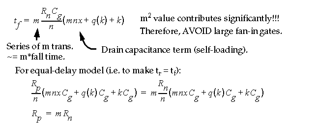
Previously, we determined that connecting two identical transistors in series will approximately double the rise or fall time of the gate.
-
Let's consider the worst case rise time for an
m
-input NAND gate (one p-transistor turns on).
-
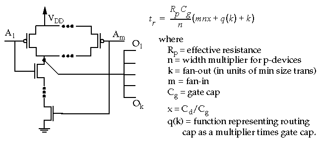
Can be reformulated in terms of C
g
as:
-
When q(k) = k, routing cap adds as much load cap as there is gate cap.
-
Might want to increase size of driving transistors to reduce effect of routing cap. (e.g. standard cells)
-
When q(k) = 0.1 -> 0.2k (circuit is dominated by self-loading), no advantage to increasing size of driving transistors. (e.g. custom layout).
-
Does this mean that the n-transistors need to be m times wider than the p-transistors?
-
In general, NANDs are a better choice than NOR gates. Why?
-
Also, the best speed performance is obtained by using gates where the number of inputs ranges between 2 and 5.
-
A classic CMOS trade-off:
-
General Guidelines:
-
Use NAND structures where possible.
-
Place inverters or small fan-in NAND gates at high fan-out nodes.
-
Avoid NOR structures in high-speed circuits, particularly with a fan-in greater than four and where fan-out is large.
-
Use a fan-out below 5-10.
-
Use minimum-sized gates on high fan-out nodes to minimize load.
-
Keep rising and falling edges sharp.
-
When designing with power and area as constraints, remember that large fan-in complementary gates will always work given enough time.
-
Guidelines to improve delay:
-
Size transistors when
routing
and
gate
capacitance contributes significantly to total load capacitance.
-
Sizing transistors along series paths can improve delay. In this case,
increase
the size of transistors proportional to their distance from the output node.
-
Order transistors so that the transistor
closest
to the
output
is the transistor that receives its input signal last.
-
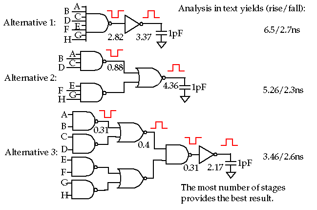
Manipulate logic expressions to replace large fan-in gates with equivalent circuits composed of gates with smaller fan-ins.
-
Insert buffers (i.e. an inverter) on the output of large
fan-in
gates in order to reduce the output load capacitance.
-
Use other styles of logic (to be discussed).
-
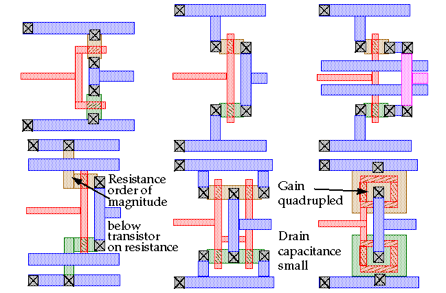
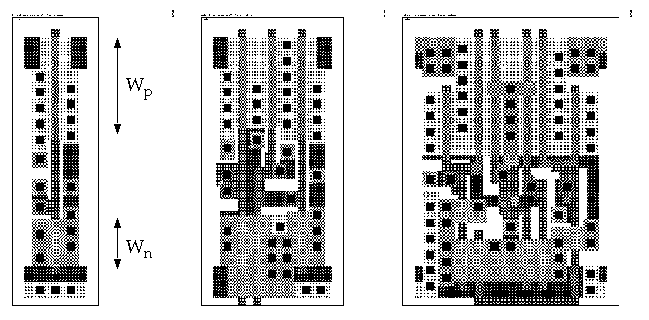
Inverter layout alternatives:
-
NOTE: A true donut "inverter" is NOT optimal:
-
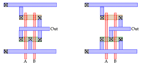
All complementary gates may be designed using a single row of n-transistors above or below a single row of p-transistors, aligned at common gate connections.
-
"Stacked layout" (on right): signals applied to multiple n- and p-transistors.
-
Works well for cascaded gates.
-
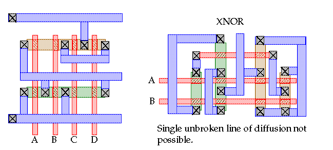
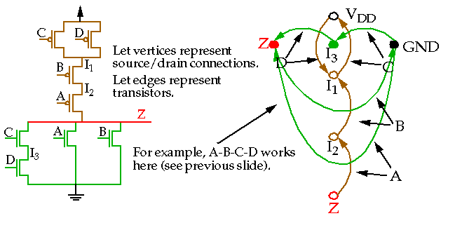
"Line of diffusion" rule:
-
Transistors form a line of diffusion intersected by poly.
-
Diffusion will be unbroken if identically labeled Euler paths can be found for the p and n trees:
-
CMOS Standard Cell Design:
-
The cells are characterized by some geometric regularity such as a fixed cell height.
-
A library of common gates such as NAND, NOR, XOR, INV, etc. that can be used by automatic place and route tools.
-
Programmable Logic Array (PLA):
-
Used when implementing complex control logic in CMOS.
-
Start with a canonical format called
two-level
sum-of-products
representation.
-
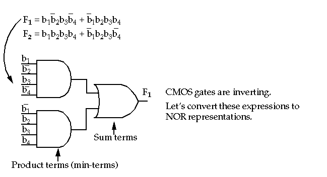
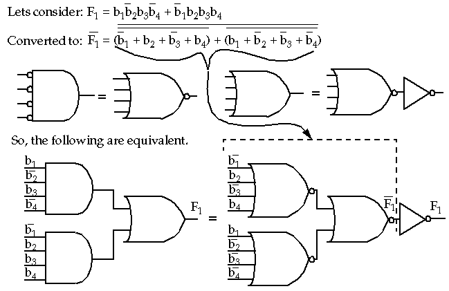
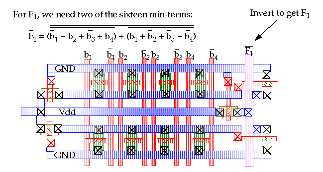
PLA: Converting to NOR-NOR format.
-
PLA: NANDs may also be used. Which do you think is faster?
-
Moreover, we want an area efficient implementation since these functions can be large.
-
Instead of building the p-tree of the NOR, let's use pseudo-nMOS.
-
PLA: Part of a 7 segment display.
-
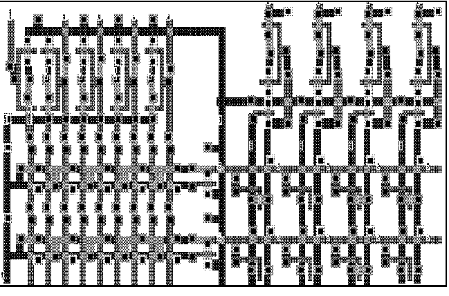
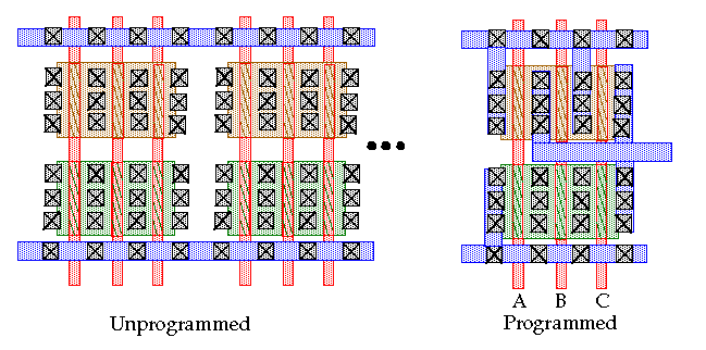
Gate Array:
-
Consists of a fixed image of under layers (typically well, diffusion and poly).
-
Wiring layers used to program the array (typically contact, metal1, via and metal2).
-
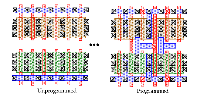
Sea-of-Gates Layout: Generalization of the Gate Array.
-
Continuous rows of diffusion are run across the entire chip.
-
Poly is tied to V
DD
and V
SS
to isolate logic gates from each other.
-
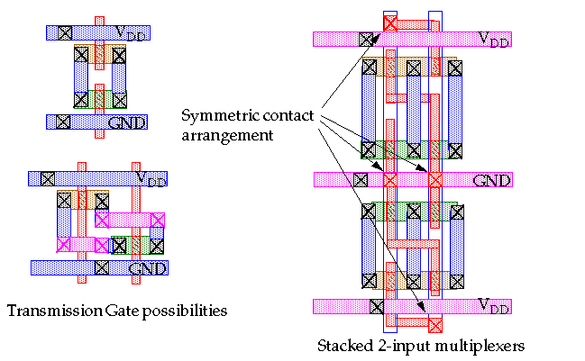
Both the control signal and its complement have to be routed.
-
It is important to equalize delays along these control lines.
-
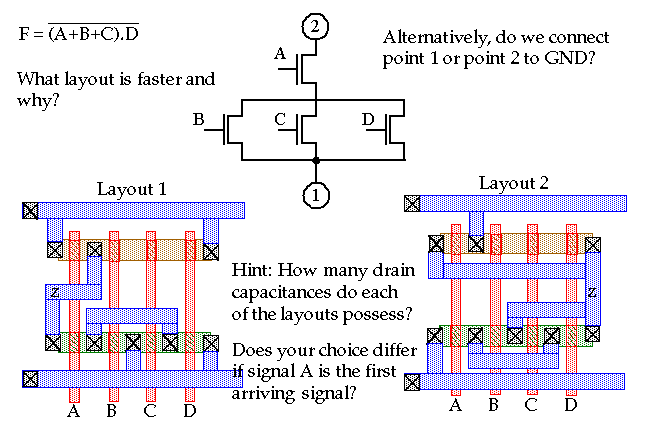
Consider the following two possible layouts.
-
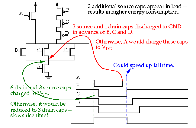
Signal arrival time scenarios.

 .
.

