-
Can be categorized into:
-
Read Write Memory
(RWM)
-
Random Access Memory (RAM): static SRAM (faster) verses dynamic DRAM (smaller) structures possible. Access time independent of physical location of data.
-
Non-RAM: Serial Access Memory (FIFO, LIFO, Shift register) and Content Access Memory (CAM). Non-uniform access time.
-
Non-volatile Read Write Memory
(NVRWM): write time much larger than read time.
-
EPROM, E
2
PROM, FLASH
-
Read Only Memory
(ROM)
-
A second classification for RAMs and ROMs:
-
Static-load: no clock required.
-
Synchronous: require a clock edge to enable memory operation.
-
Asynchronous: recognize address changes and output new data. More difficult to build.
-
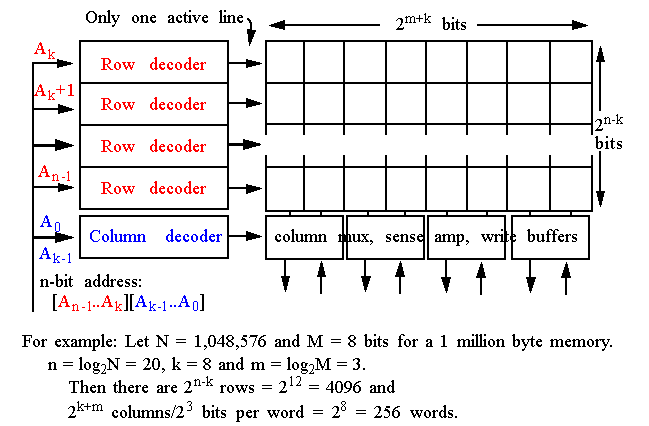
Typical memory chip architecture:
-
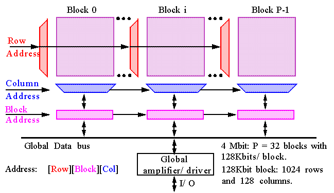
Typically, the single module version shown previously is good up to about 256Kbits.
-
For larger memories, a multiple module (P block) architecture is used.
-
ROM cells are permanently fixed: Several possibilities:
-
Virtually identical in structure to ROMs.
-
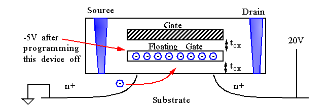
Selective enabling/disabling of transistors is accomplished through modifications to threshold voltage. This is accomplished through a floating gate.
-
Applying a high voltage (15 to 20 V) between source and drain create high electric field and causes avalanche injection to occur.
-
Hot electrons traverse first oxide and get trapped on floating gate, leaving it negatively charged.
-
This increases the threshold voltage to ~7V. Applying 5V to the gate does not permit the device to turn on.
-
The method of erasing is the main differentiating factor between the various classes of reprogrammable nonvolatile memories.
-
EPROM
:
-
UV light renders oxide slightly conductive.
-
Erase is slow (seconds to several minutes).
-
Programming is slow (5-10 microsecs per word).
-
Limited number of programming cycles - about 1000.
-
Very dense - single transistor functions as both the programming and access device.
-
EEPROM
or
E
2
PROM
:
-
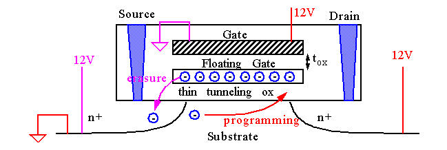
Very thin oxide allows electrons to flow to and from the gate via Fowler-Nordheim tunneling.
-
Erasure is achieved by reversing the voltage applied during writing.
-
Flash EEPROM
:
-
Combines density adv. of EPROM with versatility of EEPROM.
-
Uses avalanche hot-electron-injection approach to program.
-
Erasure performed using Fowler-Nordheim tunneling.
-
Monitoring control hardware checks the value of the threshold during erasure - making sure the unprogrammed transistor remains an enhancement device.
-
Programming performed by applying 12V to gate and drain.
-
Erasure performed with gate grounded and source at 12V.
-
SRAM: Read Operation
-
Precharging bit and bit_bar to 5V before enabling the word line would help.
-
SRAM: Read Operation:
-
Key aspect of precharge RAM read cycle: Timing of RAM addresses, the precharge pulse and the enabling of the row decoder.
-
If word assertion goes high
before
end of precharge, RAM cells on active wordline will see both lines ACTIVELY pulled high - may flip state.
-
If address changes
after
the precharge cycle has finished, more than one word line will be accessed and more than one RAM cell will have the chance to pull the bit lines down -> erroneous READ data.
-
See Weste and Eshraghian for a configuration that eliminates precharging but requires transistor ratioing and a sense amplifier.
-
Also, row and column decoder layouts and options discussed.
-
DRAM:
-
Refresh: Compensate for charge loss by periodically rewriting the cell contents.
-
Read followed by a write operation.
-
Typical refresh cycles occur every 1 to 4 milliseconds.
-
4 transistor DRAM created by simply eliminating the p tree in an SRAM cell.
-
Logic 1 values are, of course, a threshold below V
DD
.
-
Most common method of refresh is to read
bit2
, place its inverse on
bit1
and assert
write
.
-
Precharge method of 'setting'
bit2
is preferred (no steady-state current).
-
Memory structure of choice in ASICs because of its relative simplicity in both design and operation.
-
During read operation, charge redistribution occurs between node X and node bit.
-
C
x
is typically 1 or 2 orders of magnitude smaller than C
bit
so the delta-V value is typically 250 mV.
-
Most pervasive DRAM cell in commercial memory design.
-
1T DRAM observations:
-
Amplification of delta-V (through a sense amplifier) is necessary in order for the cell to be functional.
-
Other cell designs used sense amps only to speed up the read operation.
-
The read-out operation is destructive ! Output of sense amp is imposed onto the bit line with word-line high during read-out.
-
1T transistor requires an explicit capacitor (3T used gate capacitance). Capacitance must be large (~30fF) but area small - key challenge in design.
-
Bootstrapping word-line to a value larger than V
DD
circumvents V
T
loss on storage capacitor.
-
Content Access Memory (CAM):
-
Determines if a match exists between a data word with a stored word.
-
Used in Translation-look-aside buffers.


