-
Layout or Design Rules:
-
Design rules specify geometric constraints on the layout artwork.
-
Provide a communication channel between the IC designer and the fabrication process engineer.
-
Objective:
-
To obtain a circuit with optimum yield.
-
To minimize the area of the circuit.
-
To provide long term reliability of the circuit.
-
Design rules represent the best compromise between performance and yield:
-
More conservative rules increase yield.
-
More aggressive rules increase performance.
-
Design rules represent a
tolerance
that ensures high probability of correct fabrication - rather than a hard boundary between correct and incorrect fabrication.
-
Layout or Design Rules:
-
Two approaches to describing design rules:
-
Lambda-based rules: Allow first order scaling by linearizing the resolution of the complete wafer implementation.
-
To move a design from 4 micron to 2 micron, simply reduce the value of lambda.
-
Worked well for 4 micron processes down to 1.2 micron processes.
-
However, in general, processes rarely shrink uniformly.
-
Probably not sufficient for submicron processes.
-
Micron rules: List of minimum feature sizes and spacings for all masks, e.g., 3.25 microns for contact-poly-contact (transistor pitch) and 2.75 micron metal 1 contact-to-contact pitch.
-
Micron rules can result in as much as a 50% size reduction over lambda rules.
-
Normal style for industry.
-
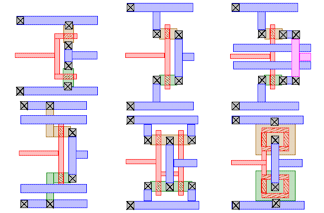
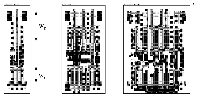
Inverter layout alternatives:
-
All complementary gates may be designed using a single row of n-transistors above or below a single row of p-transistors.
-
The right side shows a "stacked layout".
-
Works well for cascaded gates.
-
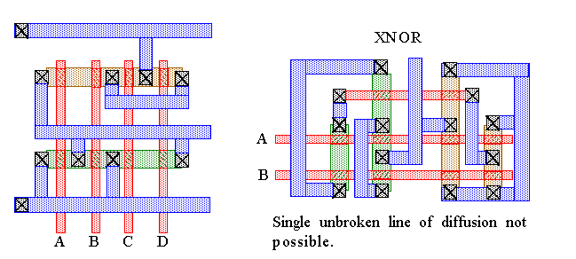
"Line of diffusion" rule:
-
Transistors form a line of diffusion intersected by poly.
-
Diffusion will be unbroken if identically labeled Euler paths can be found for the p and n trees:
-
Both the control signal and its complement have to be routed.
-
It is important to equalize delays along these control lines.
-
CMOS Standard Cell Design:
-
The cells are characterized by some geometric regularity such as a fixed cell height.
-
A library of common gates such as NAND, NOR, XOR, INV, etc. that can be used by automatic place and route tools.