-
Observations:
-
Fully restored
(V
DD
and GND) output levels results in high noise margins.
-
Ratioless
: Logic levels are not dependent on the relative device sizes.
-
Low output impedance
in steady state: increases robustness to noise.
-
High input impedance
: fanout is theoretically unlimited.
-
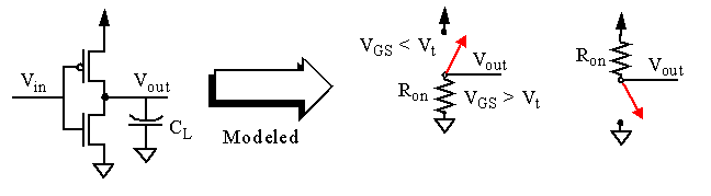
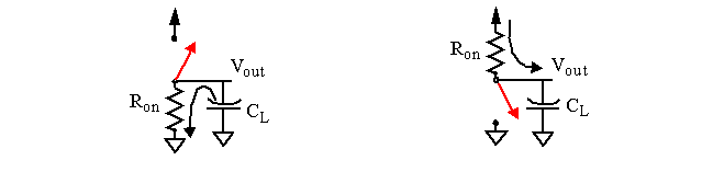
It is possible to approximate the transient response to an RC model.
-
This model assumes the transistors switch instanteously.
-
Load capacitance, C
L
, is due to
diffusion, routing
and
downstream
gates.
-
This "ideal" model predicts transient response is R
on
C
L
.
-
This indicates a fast gate is built by keeping either or both of R
on
and C
L
small.
-
Unfortunately, R
on
in the actual device is nonlinear function of the voltage across it.
-
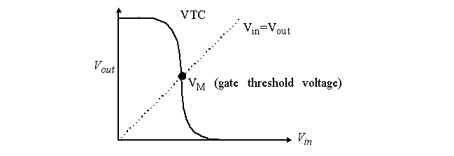
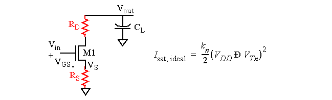
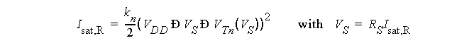
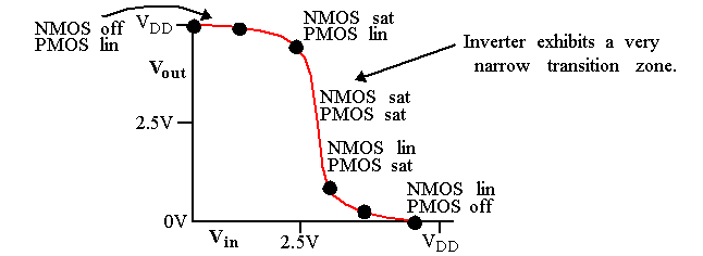
Previously, we defined V
M
as the
inverter threshold voltage
but did not derive an analytical expression for it.
-
V
M
is defined as the point where V
in
= V
out
in the VTC of the inverter.
-
In this region, both the NMOS and PMOS transistors are in saturation.
-
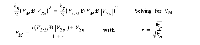
Therefore, the value of V
M
can be obtained by equating the NMOS and PMOS currents.
-
V
M
is situated in the
middle
of the available voltage swing (V
DD
/2) when k
p
= k
n
(assuming the threshold voltages are similar).
-
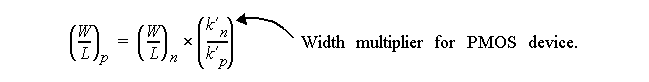
This requires sizing given by:
-
From previous analysis, this means making the PMOS three times wider.
-
Having V
M
at V
DD
/2 results in comparable low and high noise margins, which is desirable.
-
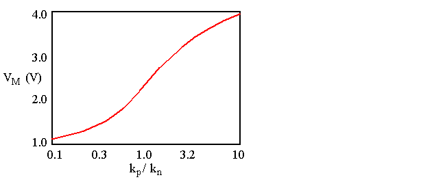
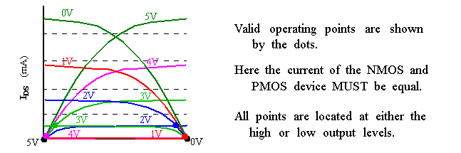
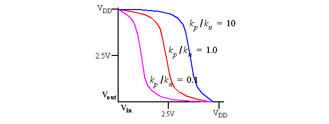
Observations from plot:
-
V
M
is relatively
insensitive
to variations of k
p
/k
n
around the center point.
-
Small variations in the ratio (0.7 -> 1.5) do not disturb the VTC much.
-
Industry sets the ratio of PMOS width to NMOS width to
2
instead of 3.
-
Secondary effects, e.g. velocity saturation, also helps with this.
-
Changing the ratio shifts the transient region:
-
Constructing an inverter with an asymmetrical VTC w.r.t. V
M
is useful in filtering noisy input low or high signals.
-
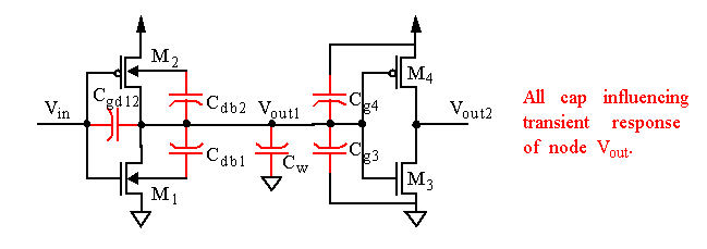
Propagation delay is determined by the time it takes to charge/discharge the load cap, C
L
.
-
Simple propagation delay models
lumps
all capacitances into C
L
.
-
In this analysis, assume V
in
is driven by an ideal voltage source with fixed rise/fall times.
-
Observations:
-
C
gd12
: Capacitance between the gate and drain of the first inverter.
-
M
1
and M
2
are either in
cut-off
or in
saturation
in steady-state.
-
It is reasonable to assume that only
overlap capacitances
contribute.
-
(Remember, gate cap is either completely between gate/bulk (cut-off) or gate/src (sat).
-
Here, in the lumped model, we will replace the C
gd12
with a capacitor to GND.
-
The value of this capacitor is given as C
gd
= 2*C
GD0
*W where C
GD0
is overlap capacitance per unit width.
-
Note it is doubled due to the
Miller effect
.
-
Observations (cont):
-
C
db1
and C
db2
: Capacitances due to the reversed biased
pn-
junction.
-
These caps are quite nonlinear (voltage dependent).
-
We linearized these caps over the voltage range of interest:
-
with C
j0
the junction cap per unit area under zero bias conditions.
-
The bottom plate and sidewall zero bias values can be obtained from the SPICE model CJ and CJSW parameters.
-
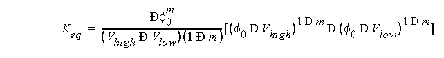
Keq was derived in an earlier lecture.
-
Consider a 1.2
m
m 5V technology and the previous inverter chain.
-
Assume
f
0
is 0.6V for both NMOS and PMOS and
m
= 0.5.
-
Let's compute C
db1
for the NMOS transistor.
-
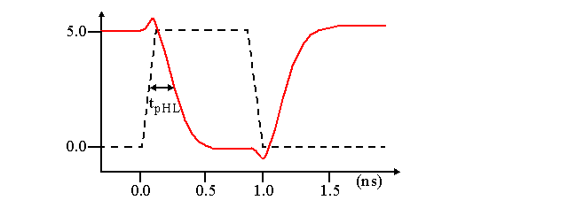
Propagation delay is computed between the 50% points.
-
This is the time-instance when V
out
reaches 2.5V.
-
For the high-to-low transition, we linearize over {5V, 2.5V} and for the low-to-high transition over {0, 2.5V}.
-
High-to-low
: V
out
is initially 5V: V
high
= -5V. At 50%, V
low
= -2.5V. K
eq
=
0.375
.
-
Low-to-high
: V
out
is initially 0V: V
low
= 0. At 50%, V
high
= -2.5V. K
eq
=
0.611
.
-
The same, but reversed, values are obtained for PMOS device.
-
Therefore, the junction capacitance can be replaced by a linear component with only minor effects on logic delays.
-
Observations (cont):
-
C
w
: The capacitance is negligible (<1fF) and can be ignored, in this case.
-
C
g3
and C
g4
: We simplify by assuming all gate cap due to
M3
and
M4
is connected between V
out
and GND (or VDD).
-
Overlap
and
gate
capacitance clustered into C
g
= C
ox
WL.
-
But what about the
Miller effect
?
-
We can safely ignore it here by assuming the driven gate's output does
not
change until
after
the 50% point of the input is reached.
-
We also assume, with minor errors, that the
channel cap
of the driven gate remains constant over this interval.
-
Text gives a good example of the capacitance calculated from the
layout
of a two-inverter chain, as shown above.
-
Loads given as
32.75fF
for high-to-low and
32.6fF
for low-to-high.
-
Computed by integrating capacitor (dis)charge current:
-
But i(v) is a
nonlinear
function of v (the voltage across the cap).
-
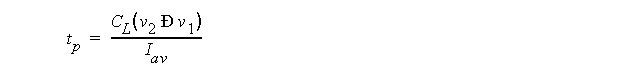
An approximation can be obtained by replacing the time-varying charging current by a fixed current I
av
.
-
This is the average of the currents at the end points of the voltage transition.
-
Calculation between the 50% points yield:
-
Low-to-high: v
1
= V
OL
and v
2
= (V
OH
+V
OL
)/2.
-
High-to-low: v
1
= V
OH
and v
2
= (V
OH
+V
OL
)/2.
-
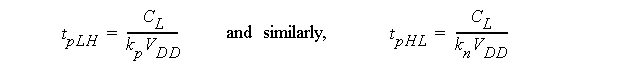
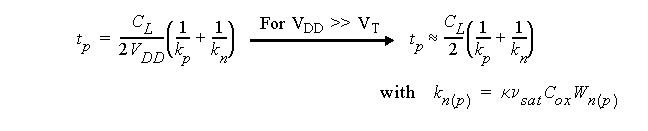
t
pLH
and t
pHL
is given by:
-
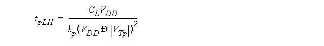
Consider t
pLH
for an inverter.
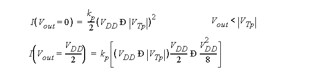
-
Assume V
in
changes abruptly from V
DD
to 0, leaving the NMOS off and the PMOS in
saturation
while V
out
< |V
Tp
|, after which it is in
linear
mode.
-
Here, V
OH
- V
OL
= V
DD
and, for I
av
, we have the boundary cases:
-
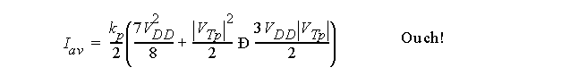
Assuming the PMOS stays in saturation, simplifies things considerably and only adds a small error (5%-8% for VDD 3-5V).
-
Here, I
av
is just the saturation expression.
-
With V
DD
assumed >> |V
Tp
|:
-
Therefore, the k
n
/= k
p
,
average propagation delay
is:
-
Minimizing propagation delay amounts to:
-
Reducing C
L
.
-
Which is composed of self-loading (diffusion) cap, routing cap and fan-out cap.
-
Increase k
p
and k
n
.
-
e.g. increase the W/L ratio of the transistors.
-
Warning: doing so
increases
the self-loading and fan-out factor, and therefore C
L
!
-
Increase V
DD
.
-
Not a design parameter. Also, trend is to reduce it to deal with
electric field density
and
power consumption
issues.
-
Text gives an analysis using a two-inverter sequence.
-
Several observations can be made from the analysis:
-
The p-transistor was made
3
times larger than the n-transistor.
-
For symmetrical high-to-low and low-to-high propagation delays.
-
This also
triples
the p-transistor gate and diffusion capacitances.
-
It is possible to speed-up the inverter by
reducing
the width of the PMOS device!
-
This increases t
pLH
but reduces t
pHL
.
-
Optimal width ratio
of PMOS to NMOS can be shown to be:
-
This reduces NM
L
a little, but it is usually acceptable.
-
NOTE: This holds true only if C
w
is negligable!
-
Half of the load capacitance is due to the inverter itself (
intrinsic
or
self-loading
) and half is due to the fan-out (
extrinsic
) gate capacitance.
-
The extrinsic capacitance
dominates
the propagation delay for large fan-outs.
-
Propagation delay increases
linearly
with the fan-out
N
:
-
with t
p
(0) and t
p
(1) the propagation delay under
0
fan-out and a fan-out of
1
, respectively.
-
Finite rise/fall time of the input signal cause both devices to remain on:
-
Here, t
pHL
increases approximately linearly with increasing rise-time values, t
r
> t
pHL
.
-
A high performance design challenge is to keep the
signal rise times
<= the
gate propagation delay
, for speed and power consumption.
-
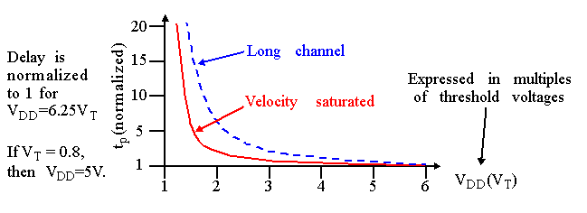
Velocity Saturation
-
Saturation (dis)charge current
proportional
to V
2
DD
previously assumed.
-
Velocity saturation makes I
av
proportional to V
DD
instead.
-
The inside curve illustrates the
lack
of a first-order dependence of t
p
on V
DD
.
-
For larger values of V
DD
, e.g., V
DD
> 4V
T
, t
p
is relatively constant.
-
For smaller values, e.g., V
DD
< 2 V
T
, a
sharp increase
in t
p
is observable.
-
In this case, the simplification used to derive the first order approximation are no longer valid.
-
Source Resistance
-
We indicated previously that R
S
and R
D
are a more accurate model.
-
Two effects of R
S
and R
D
.
-
The V
GS
of the discharge transistor is reduced (since V
S
is > 0), hence lowering the current.
-
The threshold of the transistor is increased, since the source is no longer grounded.
-
The value of R
S
ranges from
10
s of ohms to several
k
Ohms, depending on the manufacturing process and the device width.
-
Assuming a minimal size device, for 1.2 mm process, R
S
/R
D
equal 70 Ohms.
-
Here, saturation current is reduced by only 1.3% for V
DD
= 5V.
-
For a process that uses a lightly doped drain (
LDD
) approach, R
S
/R
D
~= 1-1.5k Ohms.
-
Here, saturation current is reduced by
20
% for V
DD
= 5V!
-
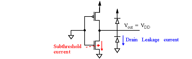
The almost ideal VTC of the CMOS inverter is
not
the main reason that high-complexity designs are implemented in static CMOS.
-
Rather, its the almost
zero
power consumption in steady-state mode.
-
The reversed-bias diode current is, in general, very small.
-
Typical values are 0.1 to 0.5nA at room temperature.
-
For a device at 5V with 1 million devices, power consumption is 0.5mW.
-
A more serious source is the subthreshold current.
-
The closer V
T
is to zero, the larger the leakage with V
GS
= 0V.
-
This establishes a firm lower bound on V
T
, which is > 0.5V today.
-
For both sources of leakage, the resulting static power dissipation is given by:
-
The junction leakage currents are caused by
thermally generated carriers
.
-
Their value
increases exponentially
with increasing junction temperature.
-
For example, 85 degrees C (a common junction temperature) results in an increase by a factor of
60
over room temperature.
-
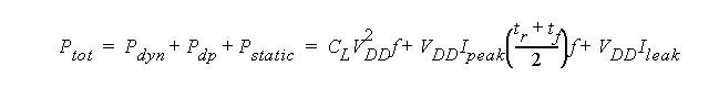
Dynamic power is much larger than static power and can be broken into 2 parts.
-
Load capacitance
, C
L
, power.
-
Power consumed via
direct path currents
(crow-bar currents).
-
C
L
power (we derived this previously):
-
Charging C
L
to V
DD
draws C
L
* V
2
DD
energy from the power supply.
-
Half of this energy is stored on the cap (C
L
*V
2
DD
/2) and later dissipated through the NMOS device.
-
So, an energy = C
L
* V
2
DD
is consumed for every L->H and H->L transition.
-
Therefore, for a clock frequency of
f
,
-
Technology advances decrease t
p
and increase
f
and C
L
(higher integration).
-
For example, at 30fF/gate at 100MHz and V
DD
= 5V, 75
m
W is dissipated per gate. With 200K gates and
a
= 20%,
3W
are dissipated.
-
1W
is consumed with 100 output pins at 20pF/pin and
f
= 20MHz.
-
One of the driving forces for lower supply voltages (
quadratic
effect).
-
For example, 5V -> 3V drops
4W
to
1.44W
(assuming the same f).
-
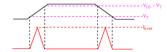
Direct-path currents.
-
Zero rise/fall times is not a realistic assumption.
-
Using triangles and V
DD
>> |V
T
|, the power consumed is
-
Avoid large values for t
f
and t
r
to minimize.
-
Direct-path power is typically only about
20%
of the dynamic power.
-
The
Power-Delay
product was also defined previously.
-
It is the energy consumed by the gate per switching event.
-
We've defined a switching event to consist of a 0 -> 1 and a 1 -> 0 event.
-
Under the condition that the static and direct-path currents are ignored.