-
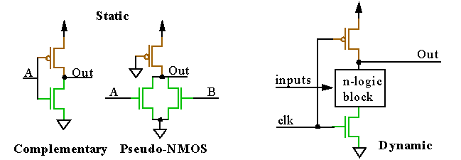
Static
:
-
At every point in time (except during the switching transient), each gate output is connected to either V
DD
or V
SS
via a low-resistance path.
-
Slower and more complex than dynamic but "safer".
-
Dynamic
:
-
Rely on the temporary storage of signal values on the capacitance of
high-impedance
circuit nodes.
-
Simplier in design and faster than static but more complicated in operation and are sensitive to noise.
-
We've already looked at full complementary design.
-
Therefore, the following must hold.
-
This condition is met if (but
not
only if) F and G are
dual
equations, e.g.,
AND
s in F are
OR
s in G.
-
Static CMOS gates inherit the nice properties of the basic
CMOS inverter
.
-
High noise margins.
-
No static power consumption.
-
Comparable rise and fall times (under the appropriate scaling conditions).
-
The last point needs further clarification:
-
This is true if the PUN and PDN networks have identical
current-driving
capabilities.
-
For the inverter, this required that p-transistors be
widened
by a factor of m
n
/m
p
.
-
This is complicated for complex gates since the current driving capabilities are determined by the values of the input signals as well.
-
As we've done in the lab, characterize based on the worst case.
-
Performing a manual analysis of the
dynamic behavior
of complex gates is only tractable via a switch model.
-
Here, the transistor is modeled as a switch with an infinite off-resistance and a finite on resistance,
R
on
.
-
R
on
is chosen so that the equivalent
RC-circuit
has a propagation delay identical to the original
transistor-capacitor
model.
-
R
on
is inversely proportional to the W/L ratio but varies during the switching transient.
-
As we did for (dis)charge currents, we estimate R
on
at the endpoints of the transitions, e.g., for t
pHL
:
-
The text gives an example using 1.2
m
m CMOS process with V
DD
= 5V.
-
R
n
is found to be 9.7 k
W
for t
pHL
and R
p
is 9.6 k
W
for a W/L
eff
of 2 and 6 respectively.
-
Deriving propagation delay can be done by analyzing the RC network.
-
Propagation delay is computed for the worst-case delay over all possible input combinations.
-
For the two-input NAND, the
worst-case
rise time occurs for
one
PMOS:
-
However, the worst-case (only) fall time occurs for two series NMOS:
-
This suggests the a
2-to-1
width scaling factor of NMOS to PMOS.
-
This analysis indicates the
deficiencies
of implementing gates with large fan-in values:
-
A gate with
N
inputs requires
2N
transistors.
-
Other circuit styles require at most
N+1
transistors, which can be a substantial advantage in area, e.g., 8 versus 5 for a 4-input gate.
-
The propagation delay of a complementary gate
deteriorates rapidly
as a function of fan-in.
-
First, the larger number of transistors increases the
overall capacitance
of the gate.
-
Second, the
series connection
in the PUN and PDN slows the gate.
-
Widening does not improve the performance as much as predicted, since widening increases gate and diffusion capacitance.
-
Fan-out in complementary gates has a larger impact on gate delay than in other circuit styles.
-
Downstream gate capacitance is always
two
per fan-out in contrast to
one
in other styles.
-
Fan-in and fan-out modeling:
-
a
1
, a
2
and a
3
are technology-dependent weighting factors.
-
The linear dependence on fan-out is easy to understand since load
increases linearly
with fan-out.
-
There is a
quadratic dependence
on fan-in since increasing fan-in raises both C
L
and (dis)charging resistance in a linear way (under no scaling).
-
Several approaches may be used to alleviate this problem:
-
Transistor sizing
-
Increasing size decreases the second-order factor in the t
p
expression.
-
However, as indicated above, if load is dominated by
intrinsic capacitance
(self-loading), propagation delay is not improved.
-
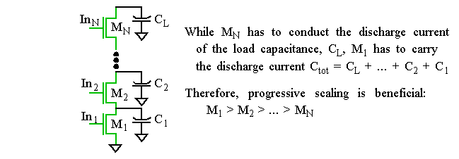
Progressive transistor sizing
-
Previous analysis lumped capacitance at the output node and
internal node capacitance
was ignored.
-
This model becomes increasingly inaccurate for large fan-in.
-
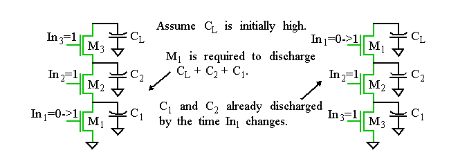
Transistor ordering
-
Not all input signals to a gate arrive at the same time.
-
Let's call the last arriving input signal
critical
, which is propagated by a
critical path
.
-
Putting the
critical-path
transistor closer to the
output
of the gate can result in a speed-up.
-
Use Another Circuit Style
-
Ratioed
-
Pass-transitor logic
-
Plus others to be discussed
-
These techniques deal with improving performance of gates with large
fan-ins
.
-
Often speed is dominated by the
fan-out
factor.
-
Scaling the transistors up in complex logic gates to drive large loads is expensive in terms of area.
-
Instead, a
buffer
(an inverter, or sequence of inverters) can be inserted between the complex gate and the fan-out.
-
Scaling is applied to the buffer transistors -- the complex gate uses minimum size transistors.


