-
An alternative to implementing complex logic is to realize it using a logic network of pass transistors (switches).
-
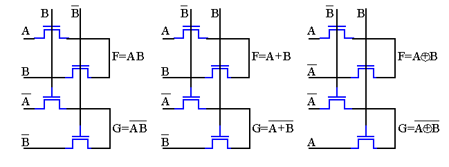
We have already observed a series connection of two switches implements AND while a parallel connection implements OR.
-
B is not redundant, it ensures a low impedance path exists when B is low.
-
Advantage: fast and simple.
-
Complex gates can be implemented using minimum number of transistors, which also reduces parasitics.
-
Static and dynamic performance depends on a switch with low parasitic resistance and capacitance.
-
Therefore, pass gate networks are often constructed from
bi-directional
transmission gates.
-
Both transistors are important:
-
Here, Mn turns off when VB reaches (5 - VTn) or approximately 3.5V!
-
Note, the VTn is increased due to the
body effect
.
-
This reduces the
noise margin
and increases
static power
dissipation.
-
Also, the
resistance
of the switch increases dramatically when the output voltage reaches Vin -VTn (linear mode).
-
The combination of both an PMOS and NMOS avoids this problem but requires that the control and its complement be available.
-
Transmission gates can implement complex gates very efficiently
-
Design Issues:
-
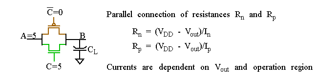
Resistance.
-
Resistance (cont).
-
During the
low-to-high
transition, the pass transistors pass through several operation modes.
-
As VGS is always equal to VDS, the NMOS is either in saturation or off.
-
The VGS of the PMOS is VDD, and the device changes from saturation to linear.
-
Vout < |VTn|: NMOS and PMOS saturated.
-
|VTp| < Vout < VDD - VTn: NMOS saturated, PMOS linear.
-
VDD -VTn < Vout: NMOS cutoff, PMOS linear.
-
It is important to incorporate the
body effect
when computing I
p
and I
n
.
-
The expression for the resistance of a pass gate
without
the body effect.
-
R
eq
is relatively constant at 10 k
W
so a
constant resistance
switch model is reasonable.
-
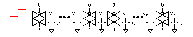
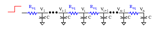
In order to analyze the response, let's replace the pass gates with R
eq
s.
-
Delay is found by solving a set of differential equations of the form:
-
Delay (cont).
-
An estimate of the dominant time constant at the output of
n
pass gates:
-
Propagation delay is proportional to
n
2
!
-
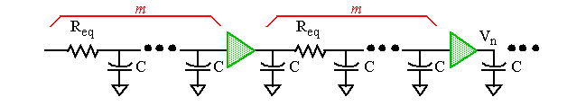
For large
n
, it is better to break the chain every
m
switches and insert buffers:
-
Total delay assuming buffer delay is t
buf
is:
-
Delay (cont).
-
Here, delay exhibits only a linear dependence on the # of switches
n
.
-
The optimal number of switches,
m
opt
, between buffers is found:
-
As t
buf
increases, the number of switches grows.
-
In current technologies,
m
opt
is typically 3 or 4.
-
For example, assume R
eq
= 10k
W
, C = 10fF, and t
pbuf
= 500ps.
-
This yields an optimal value of
m
equal to
3.8
.
-
Therefore, a buffer every 4 transmission gates is suggeste
d.
-
Transistor sizing
-
Pass gate logic family is a member of the
ratioless
logic class.
-
The dc characteristics are not affected by the sizes.
-
Performance, to the first order, is
not impacted
by changing the W/L.
-
Increasing the size reduces the resistance, but this is offset by the increase in diffusion capacitance.
-
Therefore, minimum sized devices should ALWAYS be used, unless the chain drives a significant external load capacitance.
-
In this case, increasing the sizes of the transistors from first to last in the pass gate chain will help reduce delay.
-
This is analogous to the argument given earlier for logic gate transistors close to the output.
-
Disadvantages of pass gate:
-
Requires both NMOS and PMOS, in different wells.
-
Both true and complemented polarities of the control signal needed.
-
Parallel connection of both transistors increases node capacitance.
-
Therefore, an
NMOS-only
version is advantageous.
-
Problems:
-
Reduced noise margins due to the threshold voltage drop.
-
Static power consumption.
-
One solution is to add a PMOS device, called a
level restorer
.
-
The output of the inverter is "feedback" as a control signal.
-
It turns on when the inverter output goes low (V
out
< V
DD
- |V
tp
|) and restores node
X
to V
DD
.
-
This eliminates the static power consumed.
-
However, the size of the PMOS transistor is important, since a conflict is created during switching.
-
For example, assume node
A
=0, storage node
X
=V
DD
and
B
=0->1.
-
A conducting path exists from V
DD
-M
r
-M
n
-M
3
-GND.
-
Let R
r
, R
n
and R
3
represent the resistances of transistors M
r
, M
n
and M
3
.
-
If R
r
is too small, it will be
impossible
to bring node
X
below V
M
.
-
This is called the
writability problem
, used in reference to feedback circuits.
-
Let's simplify the analysis of finding the switching point by grounding M
r
's input (open the feedback loop).
-
Assume M
r
is in
linear
mode, M
n
is in
saturation
and V
A
is close to GND.
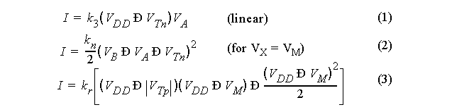
-
I is set by (3), which allows V
A
to be found via (1) and then V
B
as a function of the k-parameters (the objective).
-
Let's set the condition that V
B
< V
DD
-- in other words, some value of V
B
less than V
DD
will set V
X
< V
M
(which allows the inverter to switch).
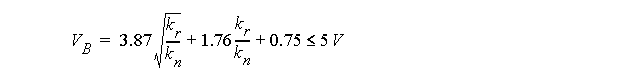
-
Assume the sizes of M
3
and M
n
are identical and V
DD
=5V, V
Tn
=|V
Tp
|=0.75V and V
M
=2.5V:
-
The boundry condition for this constraint to be valid is
m
= k
n
/k
p
> 1.55.
-
Smaller values do not allow the inverter to switch.
-
Using a value of 3 is reasonable, which amounts to making the NMOS pass gate transistor equal to PMOS restoring device.
-
What about performance?
-
Adding the level restorer increases the capacitance at V
X
.
-
Also, the rise time of the inverter is slowed due to the fight.
-
However, the fall time is improved slightly.
-
A second method of implementing NMOS-only pass gate networks is to change V
T
(if your manufacturer supports it).
-
A zero V
T
transistor for M
n
(a natural device) is one possibility.
-
This logic style is called
Complementary Pass-Transistor Logic
(CPL).
-
Properties:
-
They are
differential
circuits.
-
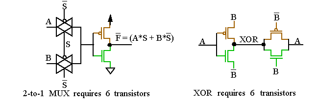
Eliminates inverters and allows minimal implementations, e.g., XOR.
-
CPL is
static
(low impedance connection to V
DD
and GND).
-
V
T
(including body effect) is reduced to below |V
Tp
|, eliminating
static power
in successor gates.
-
The design is
modular
-- all gates use exactly the same topology.
-
The main disadvantages is that turning off a zero-V
T
device is hard (plus it has a reduced noise margin).
-
Note that a 4-input NAND requires three 2-input NANDs and
14
transistors, which is >
8
!
-
The applicability of CPL is strongly dependent on the logic function to be implemented, e.g. 2-transistor XOR good for multipliers and adders.
-
CPL is extremely fast and efficient. Routing overhead is significant however.