-
Abrupt junction between
p
and
n
materials creates a concentration gradient among the carriers.
-
Electrons
diffuse
from
n
to
p
while holes diffuse from
p
to
n
.
-
The diffusion leaves behind
bound charge
in the lattice.
-
The bound charge sets up an electric field that counteracts the diffusion.
-
Electrons
drift
from
p
to
n
while holes drift from
n
to
p
.
-
Forward bias:
-
Raising potential of the
p
w.r.t
n
causes current to flow from
p
to
n
.
-
Lowers potential barrier and
diffusion
dominates
drift
.
-
Minority carriers injected into neutral region and diffuse toward plates.
-
Recombine with majority carrier causing a net flow of current.
-
Reverse bias:
-
Raising potential of the
n
w.r.t
p
causes current to flow from
n
to
p
.
-
Drift
dominates
diffusion
.
-
However, current is small since the number of minority carriers (e.g., electrons in
p
neutral region) is small.
-
For forward bias, the current is
exponentially
related to applied bias.
-
Current increases by a factor of 10 for every 60mV (2.3phi
T
) of forward bias.
-
With V
D
<< 0,
-
I
D
~= -I
S
= 10
-17
A/um
2
-
Forward Bias:
Physical basis for ideal equation:
-
Ideal diode current, ID:
-
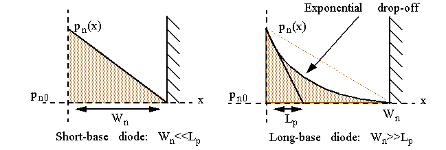
Short-base diode model
:
assumes
minority carriers
diffuse to metal contact before recombining with majority carriers.
-
The gradient of minority concentrations causes a diffusion current in neutral (bulk) regions that is proportional to that gradient.
-
The diffusion coefficients D
p
and D
n
represent the
constant of proportionality
.
-
Combining these eqs yields an expression for diode current as a function of the minority carrier conc. at the boundary of depletion region.
-
Ideal diode current, ID:
-
Law of the junction:
-
The concentration at the edge of the depletion region is an exponential function of the applied bias voltage.
-
When N
D
,N
A
>>n
i
, the equilibrium minority hole concentration in n-region is:
-
And, similarily, for the p-region is:
-
Ideal diode current, I
D
:
-
Combining (1), (2) and (3) yields:
-
Repeating this analysis for p-region and summing the current contributions yields an expression for I
D
of an ideal diode.
-
This also yields an expression for I
S
:
-
Above derivation is based on assumptions:
-
Length of neutral regions is short enough that recombination does not occur (
short-base diode
).
-
Widths of the p- and n-regions must be substantially smaller than a material constant called
diffusion length
(L
p
and L
n
).
-
Otherwise, it is a long-base diode and the minority carriers have a chance to recombine with majority carriers.
-
This only effects the W
n
and W
p
parameters in the saturation current eq.
-
Replace them with L
p
and L
n
.
-
Above derivation is based on assumptions:
-
Resistance of the neutral regions is negligible.
-
Minority carrier injection levels are substantially lower than majority concentration levels (low-injection condition).
-
Reverse Bias:
-
Ideal diode equation predicts diode current approaches the saturation current as V
D
gets much smaller than the thermal voltage.
-
Law of the junction still holds and predicts concentration of minority carriers at depletion-region approaches 0 under sufficient reverse bias.
-
Reverse Bias:
-
Diffusion of minority carriers occurs toward the junctions.
-
Electric field sweeps them across the junction to their majority zone.
-
Note: Electric field is
increased
by the reversed bias.
-
This current is limited by two factors:
-
Limited availability of minority carriers.
-
Concentration gradient does not change much once reverse-bias is sufficiently large (>4*thermal voltage).
-
Actual device reverse bias leakage is
3 orders
of magnitude higher because of the
thermal generation
of hole/electron pairs.
-
Electric field sweeps these carriers out of the region, causing an additional current component.
-
Actual device measurements are necessary to determine the value.
-
Simple models of the diode.
-
Left model based on ideal diode but is strongly non-linear and approximated by a simple model on the right.
-
Example: Assume V
S
= 3V and R
S
= 10k
W
and I
S
= 0.5X10
-16.


