-
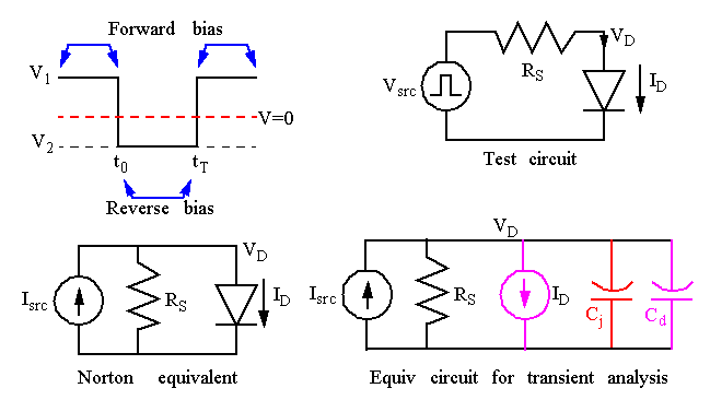
Time it takes to switch the diode between two states.
-
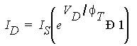
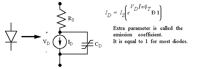
Assume R
S
is large enough that all current flows through diode in forward bias conditions.
-
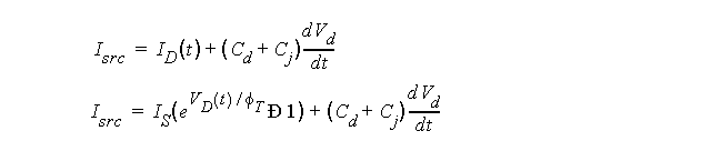
Current source I
D
is a ideal diode non-linear current source:
-
C
j
represents the space-charge (
junction capacitance
).
-
C
d
represents the excess minority carrier charge (
diffusion capacitance
).
-
(Note that both of these are small-signal capacitances; to be applicable large-signal analysis, average capacitance values must be used).
-
For Reverse bias:
-
Eliminate the current source I
D
and the diffusion capacitance C
d
.
-
Transient response requires finding a solution to:
-
Transient response:
-
The
exponential
and the
non-linear
dependence of C
d
and C
j
on V
D
make this difficult to do by hand.
-
Consider the simulated response:
-
The turn-off transient, has two operation intervals.
-
Region 1
:
-
Diode is on.
-
I
2
removes
excess minority charge
.
-
Voltage drop is small allowing C
j
to be ignored since space-charge remains ~constant.
-
Region 2
:
-
I
D
~= 0 (diode off).
-
Space-charge changes while building a reverse-bias over the diode.
-
Therefore, C
j
dominates performance.
-
Turn-off Transient.
-
Now we can derive the duration of both intervals.
-
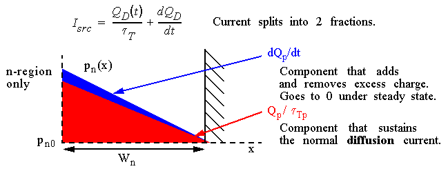
Region 1
: Removal of
excess minority charge
.
-
Charge-control expression:
-
Turn-off Transient.
-
Solving this differential equation assuming that:
-
The turn-off time is derived by solving for the time t = t
1
(Q
D
evaluates to 0):
-
Turn-off Transient.
-
Region 2
: Changing the Space Charge.
-
Diode is off, circuit evolves toward steady state.
-
During this time, a reverse voltage is built over the diode.
-
Therefore,
space charge
has to be provided.
-
The change in excess minority charge can be ignored as well as the reverse bias diode current I
d
.
-
This leaves us with a simple RC circuit (red capacitor model shown earlier).
-
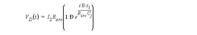
Turn-off Transient.
-
Assuming the value of V
D
at time t = t
1
is 0, the solution is the well-known exponential:
-
The 90% point is reached after
2.2
time-constants of R
src
C
j
.
-
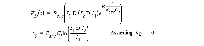
Turn-on Transient.
-
Similar considerations hold for the turn-on transient.
-
Space Charge
:
-
The transient waveform for the diode voltage (assume t = 0):
-
It takes
2.2
time constants
t
T
for Q
D
to reach 90% of its final value.
-
The lengths of the various intervals can also be estimated:
-
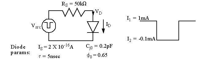
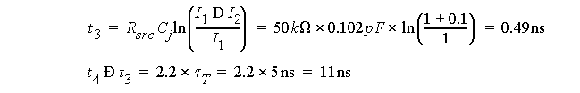
Example:
-
For (t
2
- t
1
), first compute the average
junction capacitance
C
j
assuming a voltage swing from 0 to -5V:
-
The 90% transition point is then given as:
-
The total turn-off time is 23.2 ns.
-
For turn-on:
-
The total turn-on time is 11.5 ns.
-
The faster response turn-on response is due to the larger current (1mA) available (versus the 0.1mA for turn-off).
-
The Actual Diode: Secondary effects:
-
Actual diode current is less than what is predicted by the ideal eq.
-
Not all of the applied bias voltage falls across the junction, some falls across the neutral regions.
-
However, the resistivity of the neutral regions is generally small (1 to 100 Ohms).
-
This is usually modeled with a series resistance at the contacts.
-
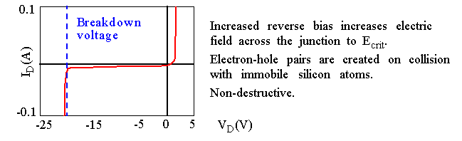
Avalanche breakdown
(MOS and bipolar processes):
-
The Actual Diode: Secondary effects:
-
For highly doped diodes, another mechanism called
Zener breakdown
can occur.
-
Operating temperature effects
:
-
The
thermal voltage
is linearly dependent upon temperature (increasing
f
T
causes the current to drop).
-
The thermal equilibrium carrier concentrations
increase
with increasing temperature causing I
S
to increase.
-
Experimentally, the reverse current doubles every 8 degrees C.
-
These have a dramatic effect on the operation of a device.
-
Current levels can increase substantially (~2X every 12 degrees C).
-
The increase in leakage current through reverse-biased diodes decreases isolation quality.
-
The SPICE diode model:
-
The preceding discussion presented a model for manual analysis.
-
If second-order effects or more accuracy (better model) is desired, simulation is required.
-
The standard SPICE model:
-
R
S
models the
series resistance
of the neutral regions (reducing current).
-
The SPICE diode model:
-
The dynamic behavior is modeled by the
nonlinear
capacitance C
D
.
-
Two different charge storage effects are combined in the diode:
-
The excess minority carrier charge
-
The space charge
-
This is nothing more than the expressions we derived earlier for C
j
and C
d
.
-
The SPICE diode model:
First-order SPICE diode model parameters
|
Parameter name
|
Symbol
|
SPICE Name
|
Units
|
Default Value
|
|
Saturation Current
|
IS
|
IS
|
A
|
1.0E-14
|
|
Emission Coefficient
|
n
|
N
|
-
|
1
|
|
Series Resistance
|
RS
|
RS
|
Ohms
|
0
|
|
Transit Time
|
tauT
|
TT
|
sec
|
0
|
|
Zero-bias Junction Cap
|
Cj0
|
CJ0
|
F
|
0
|
|
Grading Coefficient
|
m
|
M
|
-
|
0.5
|
|
Junction Potential
|
phi0
|
VJ
|
V
|
1
|