-
Can be categorized into:
-
Read Write Memory
(RWM)
-
Random Access Memory (RAM): static SRAM (faster) verses dynamic DRAM (smaller) structures possible. Access time independent of physical location of data.
-
Non-RAM: Serial Access Memory (FIFO, LIFO, Shift register) and Content Access Memory (CAM). Non-uniform access time.
-
Non-volatile Read Write Memory
(NVRWM): write time much larger than read time.
-
EPROM, E
2
PROM, FLASH
-
Read Only Memory
(ROM)
-
A second classification for RAMs and ROMs:
-
Static-load: no clock required.
-
Synchronous: require a clock edge to enable memory operation.
-
Asynchronous: recognize address changes and output new data. More difficult to build.
-
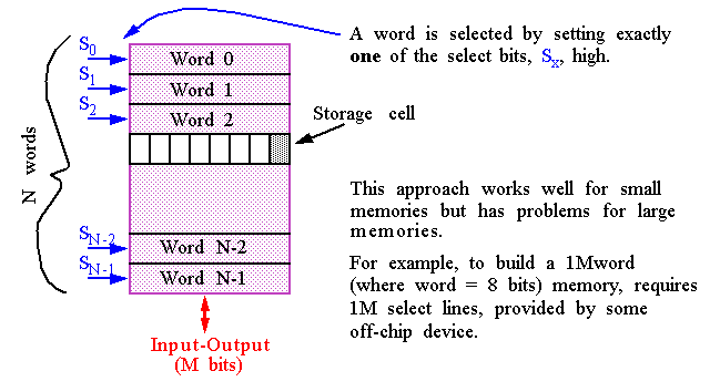
In order to build an
N-word
memory where each word is
M bits
wide (typically 1, 4 or 8 bits), a straightforward approach is to stack memory:
-
This approach is not practical.
-
What can we do?
-
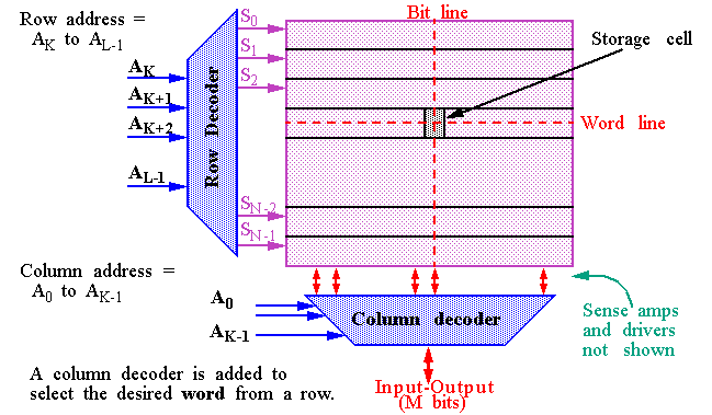
Add a decoder to solve the package problem:
-
This does not address the
memory aspect ratio
problem:
-
The memory is 128,000 time higher than wide (2
20
/2
3
) !
-
Besides the bizarre shape factor, the design is
extremely slow
since the vertical wires are VERY long (delay is at least linear to length).
-
The vertical and horizontal dimensions are usually very similar, for an aspect ratio of
unity
.
-
Multiple words are stored in each row and selected simultaneously:
-
This strategy works well for memories up to 64 Kbits to 256 Kbits.
-
Larger memories start to suffer excess delay along bit and word lines.
-
A
third dimension
is added to the address space to solve this problem:
-
For example: Let N = 1,048,576 and M = 8 bits for a 1 million byte memory.
-
n = log2N = 20, k = 8 and m = log2M = 3.
-
Then there are 2n-k rows = 212 = 4096 and 2k+m columns/23 bits per word = 28 = 256 words.
-
ROM cells are permanently fixed: Several possibilities:
-
Virtually identical in structure to ROMs.
-
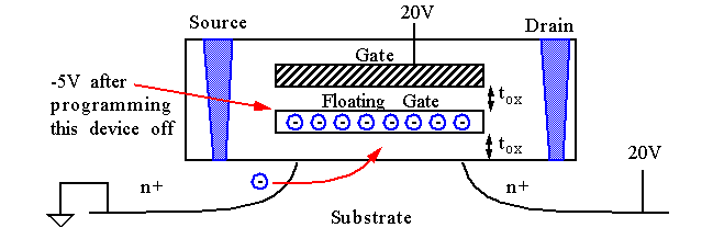
Selective enabling/disabling of transistors is accomplished through modifications to threshold voltage. This is accomplished through a floating gate.
-
Applying a high voltage (15 to 20 V) between source and gate-drain create high electric field and causes avalanche injection to occur.
-
Hot electrons traverse first oxide and get trapped on floating gate, leaving it negatively charged.
-
This increases the threshold voltage to ~7V. Applying 5V to the gate does not permit the device to turn on.
-
The method of erasing is the main differentiating factor between the various classes of reprogrammable nonvolatile memories.
-
EPROM
:
-
UV light renders oxide slightly conductive.
-
Erase is slow (seconds to several minutes).
-
Programming is slow (5-10 microsecs per word).
-
Limited number of programming cycles - about 1000.
-
Very dense - single transistor functions as both the programming and access device.
-
EEPROM
or
E
2
PROM
:
-
Very thin oxide allows electrons to flow to and from the gate via Fowler-Nordheim tunneling with VGD applied.
-
Erasure is achieved by reversing the voltage applied during writing.
-
Flash EEPROM
:
-
Combines density adv. of EPROM with versatility of EEPROM.
-
Uses avalanche hot-electron-injection approach to program.
-
Erasure performed using Fowler-Nordheim tunneling.
-
Monitoring control hardware checks the value of the threshold during erasure - making sure the unprogrammed transistor remains an enhancement device.
-
Programming performed by applying 12V to gate and drain.
-
Erasure performed with gate grounded and source at 12V.
-
SRAM: Read Operation
-
Precharging bit and bit_bar to 5V before enabling the word line improves performance.
-
DRAM:
-
Refresh: Compensate for charge loss by periodically rewriting the cell contents.
-
Read followed by a write operation.
-
Typical refresh cycles occur every 1 to 4 milliseconds.
-
4 transistor DRAM created by simply eliminating the p tree in an SRAM cell.
-
Logic 1 values are, of course, a threshold below V
DD
.
-
Most common method of refresh is to read
bit2
, place its inverse on
bit1
and assert
write
.
-
Precharge method of 'setting'
bit2
is preferred (no steady-state current).
-
Memory structure of choice in ASICs because of its relative simplicity in both design and operation.
-
During read operation, charge redistribution occurs between node X and node bit.
-
C
x
is typically 1 or 2 orders of magnitude smaller than C
bit
so the delta-V value is typically 250 mV.
-
Most pervasive DRAM cell in commercial memory design.
-
1T DRAM observations:
-
Amplification of delta-V (through a sense amplifier) is necessary in order for the cell to be functional.
-
Other cell designs used sense amps only to speed up the read operation.
-
The read-out operation is destructive ! Output of sense amp is imposed onto the bit line with word-line high during read-out.
-
1T transistor requires an explicit capacitor (3T used gate capacitance). Capacitance must be large (~30fF) but area small - key challenge in design.
-
Bootstrapping word-line to a value larger than V
DD
circumvents V
T
loss on storage capacitor.
-
Content Access Memory (CAM):
-
Determines if a match exists between a data word with a stored word.
-
Used in Translation-look-aside buffers.


