-
Variations in the I-V characteristics:
-
The current-voltage relations deviate significantly from the ideal expressions.
-
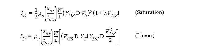
The ideal expressions are:
-
The most important reasons for this difference are:
-
Velocity saturation effects
-
Mobility degradation effects
-
Velocity Saturation:
-
We modeled carrier mobility,
m
n
, as a constant.
-
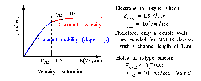
We stated carrier velocity is proportional to the electric field, independent of its value.
-
This holds up to a critical value of electric field, E
sat
, after which the velocity of the carriers tends to saturate:
-
Velocity Saturation:
-
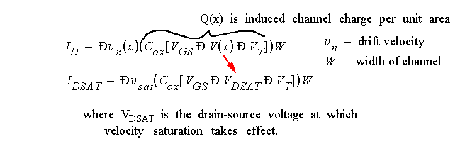
From our previous analysis of current in the linear region:
-
Current is the product of the
drift velocity
of the carriers and the available
charge
:
-
Velocity Saturation:
-
This yields a
linear
relationship between the saturation current and the gate-source voltage (contrasts the squared relationship of long-channel devices).
-
Velocity Saturation:
-
Consequently, reducing the operating voltage does
not
have such a significant effect in submicron devices as it would for long-channel devices (which is good).
-
Furthermore, I
D
is
independent of L
in velocity-saturated devices (to the first degree).
-
This suggests that current drive
cannot
be further improved by
decreasing
the channel length (as was true for long-channel transistors)(which is bad).
-
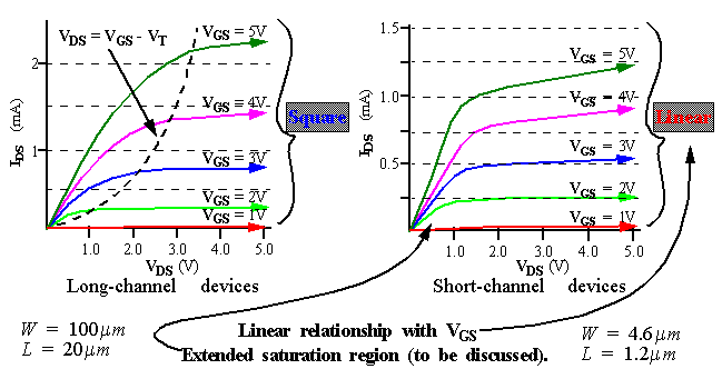
The I-V curves on the previous slide were derived from devices in the same technology (1.2um) but different sizes.
-
Long-channel device on the left has W=100um and L=20um while short-channel device on the right has W=4.6um and L=1.2um.
-
Velocity saturation
reduces the drain current by 53% for V
GS
= 5.0V and V
DS
= 5V, (1.2mA versus 2.3mA).
-
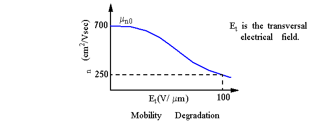
Mobility Degradation:
-
Mobility degradation
is a second effect of reducing channel-length.
-
This reduces transistor current even at "normal" electric field levels.
-
The reduction in the
electron mobility
is caused by the
vertical
component of the electric field (which was ignored before).
-
A Model for Velocity Saturation and Mobility Degradation.
-
Note that
m
n
is not a constant but is a function of the applied electric field as well (due to mobility degradation).
-
This shows that the short-channel device has an extended saturation region when compared with a long-channel device (0 <
k
< 1).
-
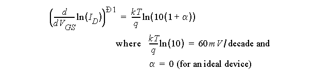
Subthreshold Conduction:
-
The transistor is partially conducting for voltages below the threshold voltage.
-
The region is referred to as
weak-inversion
.
-
Right logarithmic plot shows current decays in an exponential fashion.
-
Subthreshold Conduction:
-
In the absense of a conducting channel, the n
+
(source) - p (bulk) - n
+
(drain) terminals actually form a
parasitic bipolar transistor
.
-
The rate of decrease of current is described by:
-
Therefore, subthreshold current drops by a factor of
10
for a reduction in V
GS
of
60mV
.
-
Unfortunately, for actual devices, a is larger than 1, and current drops at a
reduced rate
.
-
Since a is a function of capacitance, it is not easily reduced (SOI).
-
Moreover, increased temperature slows the rate of decrease.
-
Subthreshold Conduction:
-
The presence of subthreshold current detracts from the ideal switch model.
-
Ideally, we want I
D
= 0 when V
GS
= 0.
-
Particularly for dynamic circuits and static power consumption (I
DDQ
).
-
This relationship puts a firm lower bound on the value of threshold voltage.
-
The slope of the previous plot in the subthreshold region is
121mV/decade
, which is equivalent to a a-factor of 1.
-
CMOS Latchup:
-
MOS technology contains a number of intrinsic
bipolar
transistors.
-
Particularly in CMOS where wells and substrates combine to form parasitic
n-p-n-p
structures.
-
Triggering these devices results in shorting V
DD
and GND.
-
This often destroys the chip, or at best, requires a power cycle.
-
NMOS src - p-substrate - n-well - PMOS src
.
-
When one of the bipolar transistors gets forward biased, it feeds the base of the other transistor.
-
Forward bias occurs when current flows through the well or substrate.
-
Positive feedback increases the current until the circuit fails or burns out.
-
CMOS Latchup:
-
R
nwell
and R
psubs
should be minimized in order to eliminate latchup.
-
This is accomplished by placing numerous well and substrate contacts close to the NMOS/PMOS devices.
-
I/O drivers should be surrounded by
guard rings
.
-
Guard rings
are just a set of well/substrate contacts arranged around the periphery of the transistor.
-
They reduce resistance and the gain of the parasitic bipolars.
-
Latchup is not a big problem today due to process innovations and improved design techniques.