-
Positive feedback is not the only means to implement a memory function.
-
A
capacitor
can act as a memory element as well.
-
In this case, a
periodic refresh
is required (in the millisecond range) due to leakage (hence the word
dynamic
).
-
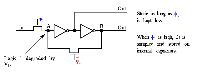
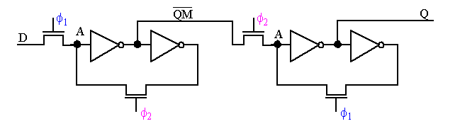
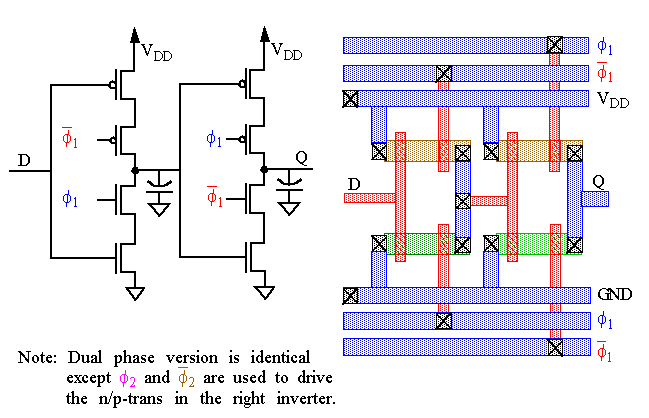
Consider the following "cheaper" (1/2 transmission gate)
positive level-sensitive
static latch as a step toward deriving a dynamic FF:
-
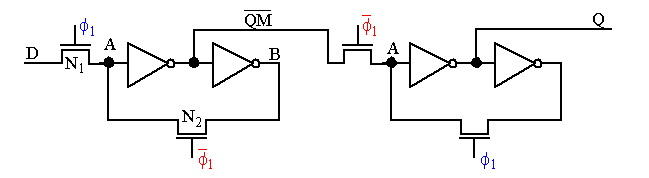
A master-slave FF is created by cascading two of these latches and reversing the clocks.
-
The problem with this latch is that f
1
and
f
1
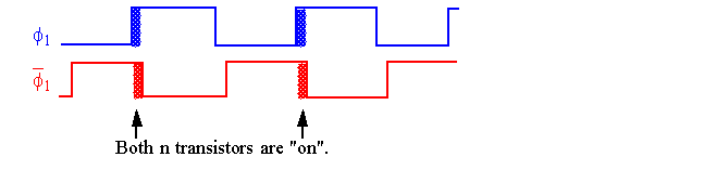
might overlap, which may cause two types of failures:
-
Node A can become undefined as it is driven by both
D
and
B
when f
1
and f
1
are both high.
-
D
can propagate through both the master and slave if both f
1
and
f
1
are high simultaneously for a long enough period (race condition).
-
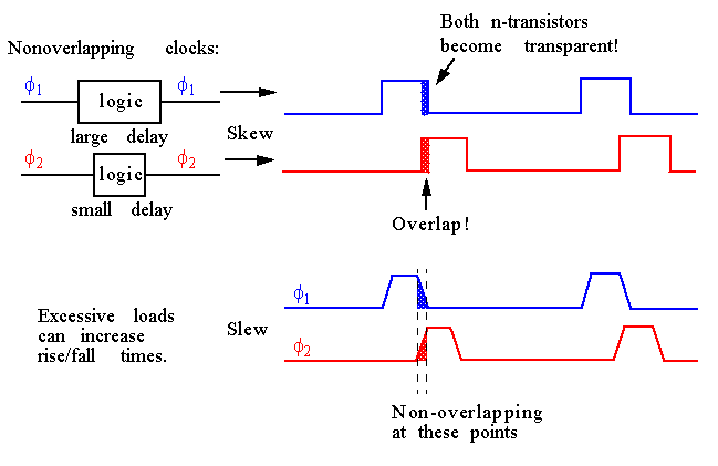
Clock skew causes conflicts and transparency.
-
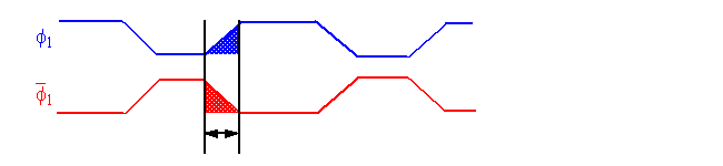
Clock slew (slow rise and fall times) can also cause transparency:
-
Clock skew is a dominant problem in current high performance designs.
-
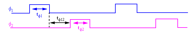
The fix is to use two non-overlapping clocks f
1
and f
2
:
-
A large t
f-12
allows proper operation even in the presence of clock skew.
-
Note that node
A
floats (dynamic) during the time period t
f-12
but is driven during t
f-1
and t
f-2 (static)
.
-
Hence, the name
pseudostatic
.
-
This version is simplier (6 trans) and is often used in pipelined datapaths for microprocessors and signal processors.
-
Disadv:
2
non-overlapping clocks
required (4 if transmission gates are used).
-
These implementations MUST be simulated at all process corners (under worst-case conditions).
-
C
2
MOS: A clever method which is
insensitive
to clock skew:
-
C
2
MOS is
insensitive
to overlap as long as the rise and fall times of the clk edges (clock slew) are sufficiently small:
-
Races
are just not possible since the overlaps activate either the pull-up or the pull-down networks but never both simultaneously.
-
The inverters force 0-1 and 1-0 propagation modes only.
-
However, if the rise and fall times of the clock are slow, there exists a time slot in which
both
n- and p-transistors are conducting simultaneously.
-
Correct operation requires the clock rise/fall times be smaller than about
5 times
the propagation delay through the FF.
-
This is not hard to meet in practical designs, making C
2
MOS especially attractive in high speed designs where avoiding clock overlap is hard.
-
The minimum allowed clock for the pipelined system is:
-
Implementation using pass-transistor based D latches
-
As indicated, races can occur when
f
and
f
overlap.
-
C
2
MOS latches can be used instead, but ONLY if the logic functions,
F
, implemented between the latches are
non-inverting
.
-
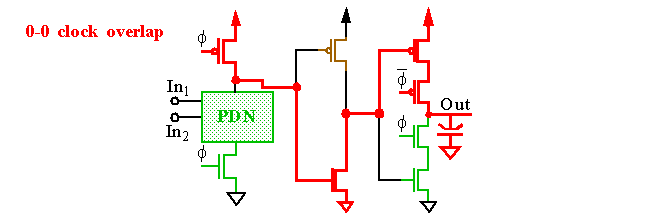
If
F
is inverting, and
f
and
f
overlap (1-1), then
C
2
is discharged as shown above.
-
NORA-CMOS
(NO-RAce) targets the implementation of fast pipelined datapaths by combining C
2
MOS with
np
-CMOS dynamic function blocks.
-
The NORA datapath consists of a chain of alternating
f
and
f
modules.
-
While one class of modules is
precharging
with its output latch in
hold mode
, the other class is
evaluating
.
-
Note that dynamic and static logic can be mixed freely.
-
Rule: # of static inversions between C
2
MOS latches should be
even
. When
dynamic
gates are present, the # of static inverters between a latch and dynamic gate and between the last dynamic gate and latch should be
even
.
-
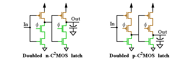
The NORA design style can be simplified so that a
single clock
is sufficient.
-
For the doubled
n
-C
2
MOS latch, when
f
= 1, the latch is in the
transparent
evaluate
mode and corresponds to 2 cascaded inverters (non-inverting).
-
When
f
= 0, both inverters are disabled (
hold
mode) -- only the pull-up network is still active.
-
The dual stage approach
completely eliminates races
.
-
This style combines the advantages of C
2
MOS and eliminates all constraints.
-
The one disadvantage is that
6
transistors (vs.
4
) are needed per latch.
-
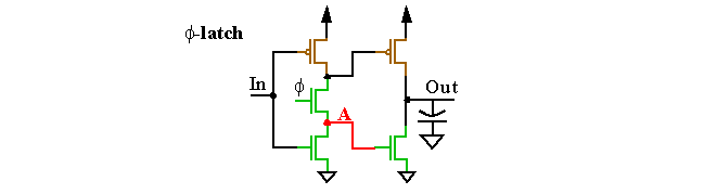
A further simplification is to control
only
the first inverter with the clock.
-
This reduces the number of transistors and the clock load is
reduced in half
.
-
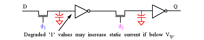
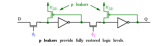
Problem: not all node voltages experience the full logic swing.
-
Node
A
(for V
in
= 0V) maximally reaches V
DD
- V
Tn
.
-
This results in a reduced drive for the output NMOS transistor and a loss in performance.
-
This design methodology is called
True Single-Phase Clock Logic
(TSPC).
-
It allows for the implementation of dynamic sequential circuits with a single clock.
-
Split-output
version reduces clock load in half, while performing well.
-
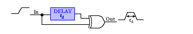
A circuit that generates a pulse of a
predetermined width
every time the circuit is triggered by a pulse or transition event (
one-shot
).
-
The circuit has
only one stable state
-- the quiescent state.
-
The trigger causes the circuit to go temporarily into a
quasi-stable
state.
-
It returns to its quiescent state after a time period determined by the circuit parameters.
-
Useful for
address transition detection
(ATD) to generate timing in static memories for subsequent operations.
-
We've seen this version in edge-triggered FFs.
-
A second class uses feedback combined with an
RC timing network
to generate a pulse of fixed width.
-
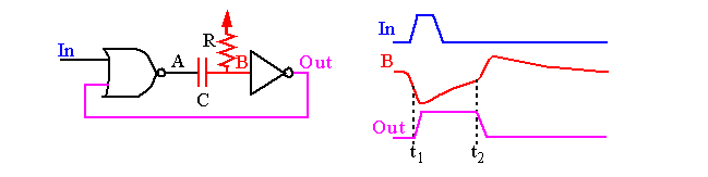
Initially,
In
and
Out
are low and therefore
A
is high.
B
is high via resistor R.
-
Pulsing
In
high causes
A
to go low, pulling node
B
with it.
-
Node
B
gets pulled high again with time constant RC.
-
Out
goes low when
B
reaches V
M
, which causes
A
to go high again (note
In
has already gone low again).
-
The width (t
2
- t
1
) is determined by the time-constant RC and V
M
.
-
Unfortunately, V
M
is relatively sensitive to process variations.
-
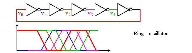
A circuit with
no stable states
.
-
The output oscillates back and forth between two
quasi-stable
states with a period determined by circuit parameters.
-
The main application of such a circuit is
on-chip clock generation
.
-
We already looked at the
ring oscillator
as an example.
-
The period T of the oscillation is:
-
where t
p
is the propagation delay of the composing gates.
-
By tapping the ring oscillator at different stages, a wide range of clock signals with different duty-cycles and phases can be derived.
-
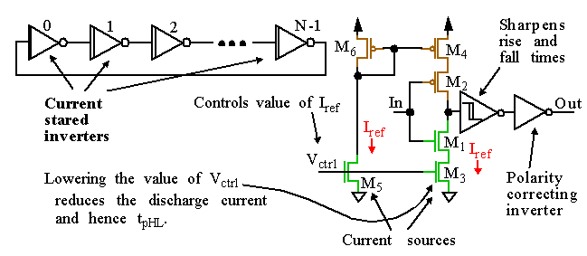
It is often desirable to tune the frequency of oscillation.
-
An example is a
Voltage-controlled Oscillator
(VCO), whose frequency is proportional to the value of a control voltage.
-
Charging current is controlled via M
5
.
-
I
ref
is translated into a charging current through the
current mirror
M
6
- M
4
.
-
Here, M
6
acts as a
diode
and sets a bias voltage V
GS6
, that is controlled by I
ref
.
-
With V
GS4
= V
GS6
and both devices operating in
saturation
, I
DS4
= I
DS6
= I
ref
.
-
Since both M
3
and M
5
operate in
saturation
, a quadratic relation exists between V
ctrl
and I
ref
(and t
p
).
-
This allows the frequency of the VCO to be controlled over a large range.
-
A Schmitt trigger is used to
sharpen
the weakened rise and fall times of the
current-stared inverter
.
-
Note that transistors M
5
and M
6
can be shared over all inverters in the chain.