-
Failure mode
is used in reference to the manifestation of a "defect" at the
electrical level
.
-
Failure modes are modeled as
faults
at logic or behavioral level of abstraction.
-
Defects are due to
failure mechanisms.
-
It is important to derive the
principal failure mechanisms
of a process.
-
Some examples include:
-
Gate oxide breakdown.
-
Incomplete contact and via fills.
-
Electromigration.
-
Wire bonding failure.
-
These
mechanisms
are tied to variations in the fabrication process:
-
Random fluctuations in the actual environment, e.g.,
-
Turbulent flow of gases used for diffusion and oxidation.
-
Inaccuracies in the control of the furnace.
-
Variations in the physical and chemical parameters of the material, e.g.,
-
Fluctuation in the density and viscosity of the photoresist.
-
Water and gas contaminants.
-
Extra and Missing Material
:
-
Can be caused by
dust particles
on the mask, wafer surface or processing chemicals, e.g. photoresist.
-
During photolithography, these particles lead to
unexposed
photoresist areas, leading to:
-
Unwanted material
or
unwanted etching
of the material.
-
Causes
shorts
and
opens
in the poly, active or metal layers.
-
Gate-Oxide-Shorts
-
Pinhole defects are common thin-ox defects, that are caused by:
-
Insufficient oxygen at the interface of Si and SiO2.
-
Chemical contamination.
-
Nitride cracking during field oxidation.
-
Crystal defects.
-
Imperfections in a uniform growth pattern of the thin oxide layer.
-
Particulate contamination in the thin oxide mask.
-
Gate-Oxide-Shorts
(cont.)
-
A
GOS
can also be created in post fabrication procedures and
operational conditions
:
-
Electric field stress due to scaling feature size without scaling supply voltage.
-
Electro-Static discharge (
ESD
).
-
Trapping of charge introduced by hot electrons.
-
May develop later due to an effect called Time Dependent Dielectric Breakdown (
TDDB
).
-
Electromigration
-
One of the major failure mechanisms in interconnects.
-
Aluminum has a low melting point, and high current densities can displace metal atoms.
-
Scaling is reducing the
Mean Time To Failure
(MTTR), which is:
-
Proportional to the width and thickness of the metal lines.
-
Inversely proportional to the current density.
-
Complete defect characterization is difficult.
-
New failure mechanisms or old ones that become more prevalent through scaling make this a challenging problem.
-
Shorts can occur:
-
Between metal lines and V
DD
or V
SS
.
-
Between subnets as bridging defects.
-
And as Gate-Oxide-Short (
GOS
) to the source, drain or channel region of the transistor.
-
Via punch-through, parasitic transistor leakage and defective pn junctions.
-
The type of fault behavior depends on:
-
The location of the short (gate-to-channel vs. gate-to-source/drain).
-
The type of the affected transistor (n or p).
-
The resistance of the short and the state of the driving transistors.
-
GOS
can exhibit
pattern-dependent
fault behavior:
-
In this circuit, two of the possible faults include a
slow-to-fall
delay fault or
SA1
fault on node
y
.
-
Test Pattern that provokes the fault
AB
= (
10
,
11
).
-
However, several test patterns can set node
A
to 1:
IJ
= (
01
,
10
,
00
).
-
This requires attention to inputs that are not directly connected to the Gate-Under-Test (GUT), which ATPGs typically do not consider.
-
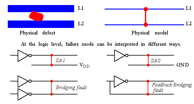
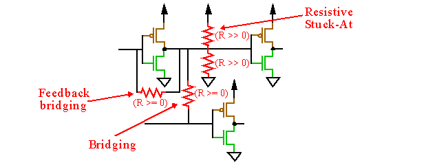
Bridges can be defined as undesired electrical connections between two or more lines in an IC, resulting from extra conducting material or missing insulating material.
-
Bridging defects may also develop after fabrication as a result of mechanisms including:
-
Oxide surface conduction.
-
Lateral charge spreading.
-
Electromigration.
-
For Bridges:
-
Fault detection
requires the test vector to set the shorted nodes to opposite logic polarities.
-
For
test generation
, physical layout information must be used to reduce the n
2
node pairings.
-
Failure modes include:
-
If one node is able to dominate the other, a
logical fault
may occur at the weaker of the two nodes.
-
If the resistance of the bridge is large enough (allowing the nodes to assume different potentials) then a
delay fault
may result.
-
If the resistance of the bridge is small enough, the defect may significantly increase the magnitude of the
steady state current
.
-
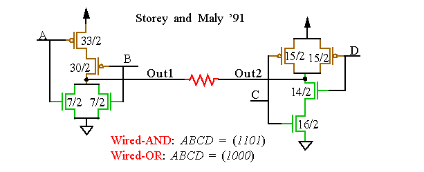
A
wired-AND
/
-OR
model used in TTL and ECL is not always applicable for CMOS.
-
Wired-AND
models the shorted nodes at 0 unless both are driven to 1.
-
Wired-OR
models the shorted nodes at 1 unless both are driven to 0.
-
For CMOS, the faulty voltage value is dependent on both:
-
The
relative strengths
of the pull-up and pull-down transistors.
-
The
number
of transistors that are
activated
in the conflicting network.
-
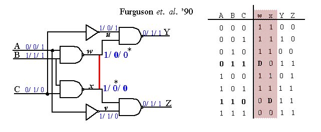
Even when a
wired-AND
fault behavior is assumed, it may not be possible to produce a test that causes a logic fault.
-
Delay fault on node
Z
results under the test sequence:
-
However, no logic fault occurs under either test that causes
w
and
x
to acquire different values:
-
ABC
= (
011
) and (
110
)
-
Defined as opens or breaks caused by missing conducting material or by extra insulating material.
-
Opens
in CMOS circuits are difficult to detect.
-
The fault behavior caused by an
open
is dependent on:
-
Its location.
-
Its resistance.
-
Its width.
-
The values of parasitic coupling capacitances and leakage currents associated with the floating node.
-
Most fault models assume:
-
The
width
of the open is large enough to prevent capacitive coupling interactions with neighboring nodes.
-
The effects of
leakage currents
are negligible.
-
Leakage current, for example, make faults
timing-sensitive
, adding test application rate as a constraint for detection.
-
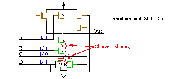
Effects such as
charge sharing
make detection difficult even when it is assumed that leakage currents are negligible and the width of the break is large.
-
Charge sharing
refers to the redistribution of charge stored at an isolated node.
-
Test
ABCD
= (
0111
,
1101
) designed to test
Stuck-Open
defect between
N2
and
N3
.
-
The same is true for
path redundancy
:
-
Path redundancy
describes a circuit configuration in which multiple independent paths drive an output node.
-
Operated functionally correct but is slower and may increase steady-state current.
-
Fault effects can be
time-dependent
for:
-
Narrow (tunneling) opens (< 0.1um).
-
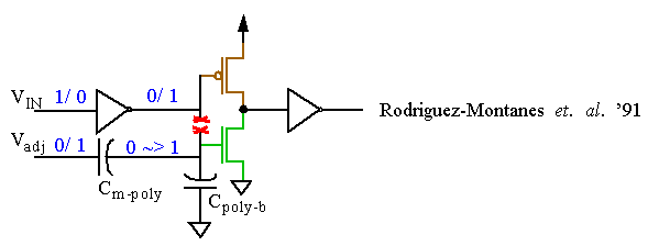
Opens in which coupling capacitance interactions and leakage currents effect the state of the node.
-
Capacitively coupled open nodes can allow the circuit to operate correctly but more slowly.
-
Also,
leakages
through the source and drain junctions can allow an output node to change state, given enough time.
-
ICs can fail at different stages of its lifetime:
-
Infant mortality
: defects that escape detection.
-
Burn-in
is designed to screen these types of defects.
-
Wear-out
: Characterized by an exponential increase in failures.
-
Main factor causing wear-out is
excessive heat dissipation
.
