-
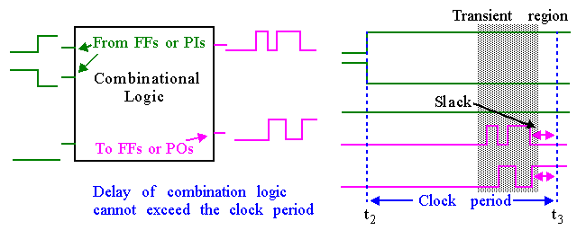
Delays along every path from PI to PO or between internal latches must be less than the operational system clock interval.
-
We have already discussed a number of defects that can cause delay faults:
-
GOS defects
-
Resistive shorting defects between nodes and to the supply rails
-
Parasitic transistor leakages, defective pn junctions and incorrect or shifted threshold voltages
-
Certain types of opens
-
Process variations can also cause devices to switch at a speed lower than the specification.
-
An SA0 or SA1 can be modeled as a delay fault in which the signal takes an "infinite" amount of time to change to 1 or 0, respectively.
-
Passing stuck fault tests is usually not sufficient however for systems that operate at any appreciable speed.
-
Running stuck-at fault tests at higher speed can uncover some delay faults.
-
Delay tests consist of vector-pairs.
-
All input transitions occur at the same time.
-
The longest delay combinational path is referred to as the critical path, which determines the shortest clock period.
-
A delay fault means that the delay of one or more paths (not necessarily the critical path) exceeds the clock period
-
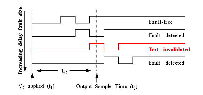
Test Definition:
-
At time t
1
, the initializing vector of the two-pattern test, V
1
, is applied through the input latches or PIs and the circuit is allowed to stabilize.
-
At time t
2
, the second test pattern, V
2
, is applied.
-
At time t
3
, a logic value measurement (a sample) is made at the output latches or POs.
-
The delay test vectors V
1
and V
2
may sensitize one or more paths, p
i
.
-
Let:
-
T
C
=
(t
3
- t
2
) represent the time interval between the application of vector V
2
at the PIs and the sampling event at the POs
-
The nominal delay of each of these paths be defined as pd
i
.
-
The slack of each path be defined as sd
i
= T
C
- pd
i.
-
This is the difference between the propagation delay of each of the sensitized paths in the nominal circuit and the test interval.
-
Difficulties with delay fault test generation:
-
Test generation requires a sensitized path that extends from a PI to a PO.
-
Path selection heuristics must be used because the total number of paths is exponentially related to the number of inputs and gates in the circuit.
-
The application of the test set must be performed at the rated speed of the device.
-
This requires test equipment that is capable of accurately timing two-vector test sequences.
-
The detection of a defect that introduces an additional delay, ad
i
, along a sensitized path is dependent on satisfying the condition:
-
ad
i
> sd
i
(or pd
i
+ ad
i
> T
C
)
-
Therefore, the effectiveness of the delay fault test is dependent on both the delay defect size and the delay of the tested path.
-
A path sensitized by a delay test consists of on-path nodes and off-path nodes.
-
The nodes along the sensitized path are referred to as on-path nodes.
-
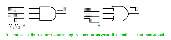
Static sensitization defines the case when all off-path nodes settle to non-controlling values (0 for OR/NOR, 1 for AND/NAND) following app. of V2.
-
This is a necessary condition to test a path for a delay fault.
-
The gates along the sensitized path have exactly one on-path input and zero or more non-controlling off-path inputs.
-
Delay fault tests are classified according to the voltage behavior of the off-path nodes.
-
Such tests can be invalidated under certain conditions.
-
Hazards can invalidate tests:
-
Static hazard: describes a circuit condition where off-path nodes change momentarily when they are supposed to remain constant.
-
Dynamic hazard: describes a circuit condition where off-path nodes make several transitions when they are supposed to make a single transition.
-
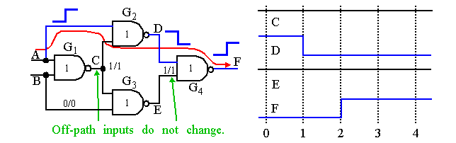
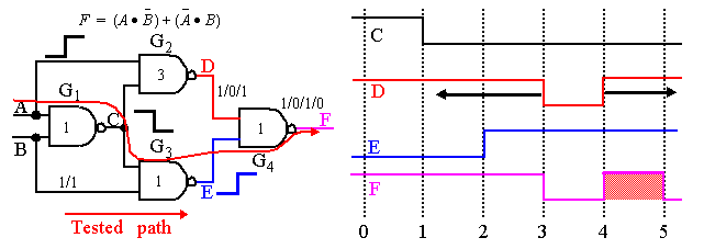
Two vector sequence is ABC = (111), (101).
-
Gate G
1
introduces an additional delay of 1 unit.
-
Output
E
of gate G
3
is driven to a logic 1, one time unit behind
D
-> 0.
-
Produces a glitch on F.
-
Two vector sequence is
AB
= (
01
), (
11
).
-
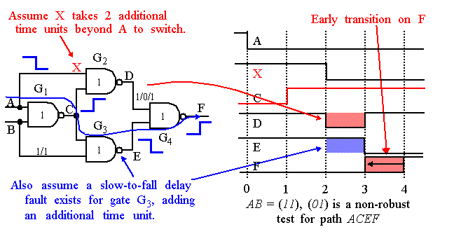
Gate G
2
has a delay value of 3 time units, due either to a defect or a different physical implementation of the NAND gate.
-
Static hazards can create dynamic hazards along tested paths and need to be considered during test generation.
-
Note, unlike the previous example, the glitch occurs before the intended transition in this case, and can invalidate the test (e.g. fault is not detected).
-
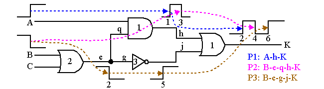
The critical path(s) of this circuit is 6 time units.
-
Let's set the clock period T = 7.
-
Assume only one faulty path.
-
No delay fault is detected if path delay along P3 is less than 7 units.
-
This test will not detect single delay faults along paths P1 or P2.
-
Assume there can be multiple faulty paths.
-
Assume P2 and P3 are faulty and P2 extends the "static glitch" at the output beyond 7 units, then it masks P3's delay fault.
-
This test is called a non-robust test for delay fault P3.
-
Each of the paths in a circuit can be classified:
-
Hazard-free robust testable
-
Robust testable
-
Non-robust testable
-
Non-robust testable but not redundant
-
Redundant
-
Off-path inputs are stable and hazard-free throughout the test interval, T
C -- m
ost desirable test since invalidation is not possible.
-
Hazard-free robust tests are desirable but it's not possible in many cases to generate them.
-
Transitions that occur at fan-out points often reconverge as off-path inputs along the tested path.
-
However, robust tests are still possible even when static hazards are present on the off-path inputs.
-
Static hazards are necessary but not sufficient to make a delay test non-robust.
-
A delay test is a robust test if the on-path nodes control the
first
occurrence of a transition through all gates along the tested path.
-
This ensures that a delay test is not invalidated or a path delay fault masked by delay characteristics of gates not on the tested path.
-
A robust path-delay test guarantees to produce an incorrect value at the output if the delay of the path exceeds the clock period, irrespective of the delay distribution in the circuit.
-
This test is robust since
F
will not change state until the transition on
E
has occurred.
-
In other words, any assignable delay to
D
can never mask a delay fault that may occur on the tested path.
-
This is true because the on-path node
E
holds the dominant input value on gate G
4,
and therefore determines the earliest transition possible on
F
.
-
Therefore, D is allowed to delay the transition on F but not speed it up.
-
It is possible that:
-
D
can cause a transition to occur on
F
after the transition on-path node
E
has occurred.
-
D may further delay the transition of
F
since it too can hold the dominant input value on gate G
4
.
-
The former condition is sufficient to cause a glitch on
F (as shown)
.
-
The latter condition implies that a robust test does not require the sensitized path to dominate the timing, or, to be the last transition to occur on all gates along the sensitized path.
-
An on-input node will make the transition either:
-
From the dominant input state of the gate to the non-dominant input state.
-
From the non-dominant input state of the gate to the dominant input state.
-
For the first case, the off-path inputs of the gate must behave in either one of two ways.
-
If the off-path input node changes state, then it must make a transition from the dominant to the non-dominant input state of the gate.
-
If it does not change state, then it must remain in steady-state at the non-dominant value during the entire test interval.
-
When all off-path inputs honor these constraints, the outputs of the gates along the test path will not make the transition until the last of all transitioning input lines have toggled.
-
For the second case, the off-path inputs must remain at their non-dominant states during the entire test interval.
-
No off-path transition is allowed.
-
In either case, hazards will not be visible at the output until after the desired transition has propagated along the tested path.
-
However, for many circuits, even this weaker set of constraints permits only a small percentage of path delay faults to be robust tested.
-
A non-robust tests allow the output to change before the on-path transition propagates along the tested path.
-
A non-robust test cannot guarantee the detection of a delay fault along a test path in the presence of other faults.
-
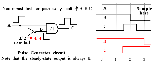
Although the delay fault introduced by the inverter is detected (as shown), a delay fault along A-C may cause the output to remain at 0 or it may push the pulse beyond T = 3 -- which invalidates!
-
A non-robust path delay test guarantees the detection of a path-delay fault only when no other path delay fault is present.
-
Single fault assumption (similar to the Stuck-At fault model).
-
The fault is called a singly-testable path-delay fault in cases where a test exists.
-
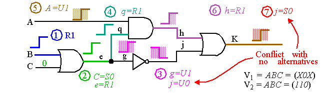
To generate test for falling transition on path P3:
-
This test is a robust, i.e., it cannot be invalidated irrespective of P2's delay.
-
Non-robust tests only require static sensitization (arbitrary values for V1).
-
There are no alternatives to generate the previous test, so we are stuck with a non-robust test for the rising transition of P2.
-
Note that in circuits with reconvergent fanout, backtracking is frequently necessary.
-
Single input change (SIC): a simpler method of generating non-robust tests.
-
Use a combinational ATPG algorithm to statically sensitize the entire path for V2.
-
V1 is obtained by changing one bit in V2 that corresponds to the origin of the path.
-
Validatable non-robust tests
-
It is desirable to find as many robust tests as possible.
-
The presence of robust tests for some paths improves the reliability of non-robust tests for other paths.
-
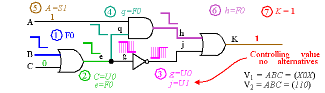
For example, there are 6 robustly testable paths in the previous circuit.
-
With these tests, the rising transition test of P2 as good as a robust test.
-
Some robust untestable paths are not even non-robust testable paths.
-
This path has no delay test.
-
A path for which both rising and falling PDFs are singly (i.e. non-robustly) testable is called a testable path.
-
A path that has one singly testable and one singly untestable PDF is called partially testable path and may be associated with a redundant fault.
-
The fault q SA1 in our circuit is redundant -- AND gate can be removed.
-
When no non-robust test exists for both paths, its singly-untestable path.
-
This path can be eliminated by circuit transformations.
-
The delay along false paths cannot affect the output transition time.
-
Unfortunately, singly-untestable PDFs are not always false paths.
-
It's possible to multiple singly-untestable PDF to be co-sensitized and for them to affect the circuit timing, if all have excess delays.
-
These paths belong to the classes multiply-testable PDFs and functionally sensitizable PDFs.
-
This is why the delays of paths whose PDFs are untestable are still taken into account while determining the clock period of the circuit.
-
A point in favor of static timing analysis.