-
The number of paths can be an exponential function of gates.
-
Parallel multipliers are notorious for having huge numbers of paths.
-
It is possible to efficiently count paths in spite of this however.
-
Directed acyclic graph (DAG) path graph for this circuit:
-
Vertices represent the PIs, POs and gates, edges represent signal flow.
-
Source and sink nodes are added to point to PIs and POs respectively, algorithm visits each node, follows it edges and adds one to destination nodes.
-
Since the maximum indegree is O(N), worst case complexity is O(N2).
-
Path-delay fault model
-
Segment-delay fault model
-
Transition fault model
-
Line-delay fault model
-
Gate delay fault model
-
They are distinguished by the size of the delay fault taken into consideration and the assumptions made concerning the distribution of delay defects.
-
We described the path-delay fault (PDF) model characteristics:
-
Two PDFs for each physical path (rising and falling).
-
Total number of paths is exponential function of number of gates.
-
Critical paths, identified by static timing analysis, must be tested.
-
Robust tests are preferred, but some paths have only non-robust tests.
-
Three types of PDFs:
-
Singly-testable PDF: has a non-robust or robust test.
-
Multiply-testable PDF (functionally testable PDF): a set of singly untestable faults that has a robust or non-robust test.
-
Untestable PDF: a PDF that is neither singly or multiply testable.
-
Segment-delay fault model:
-
A segment of an I/O path is assumed to have large delay such that all paths containing the segment become faulty.
-
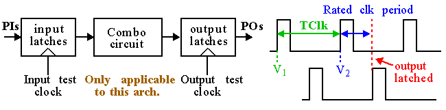
Transition fault model:
-
Faults are modeled at the gate I/Os as slow-to-rise (STR) and slow-to-fall (STF) faults that elicit
Stuck-At
type fault behavior at the POs.
-
For detection of a slow-to-rise fault, start with a SA0 fault on the line.
-
This sets the line to 1 and propagates the state of the line to a PO.
-
Let this be vector V2 then define V1 as a vector that sets the line to 0.
-
ATPG algorithms generate pairs of test vectors designed to determine which paths in the circuit can not propagate transitions.
-
Transition fault model (cont.):
-
We discussed Stuck-Open
defects that exhibit memory behavior.
-
Two vector tests were required -- an initialization pattern and a test pattern that drives the output (generates a transition) to the opposite value.
-
The transition fault model can be used to determine
Stuck-Open
fault coverage of a test set.
-
Basic assumption is that the faulty delay is large since the observation path may be (and often is) a short path.
-
Plus hazards are not taken into account.
-
Transition faults can detect localized (spot) delay defects of large (gross) delay amounts.
-
They are not reliable at detecting delay defects that are distributed.
-
Transition fault model (cont.):
-
Number of tests is upper bounded by twice the number of lines.
-
Tests are easy to generate, i.e., a stuck-at fault test generator can be easily modified.
-
Circuits with high stuck-at fault coverage usually have high transition fault testability.
-
Transition fault tests are usually augmented by some path delay tests, e.g. those that test critical paths.
-
Line-delay fault model:
-
A transition fault tested through the longest delay path.
-
Two faults per line/gate, tests are dependent on modeled gate delays.
-
Gate-delay fault model:
-
A gate is assumed to have a delay increase of a certain amount (called fault size) while all other gates retain some nominal delay.
-
Gate-delay faults only of certain sizes may be detectable.
-
The application of delay tests depends on the type of circuit and the DFT hardware used.
-
Slow-clock combinational test
-
Enhanced-scan test
-
Normal-scan sequential test
-
Variable-clock non-scan sequential test
-
Rated-clock non-scan sequential test
-
Slow-clock combinational test
-
Note that V1 is applied at a slower rate and the circuit is allowed to stabilize.
-
Enhanced scan test
-
Applicable to scan types of sequential circuits.
-
Similar to the previous method, any arbitrary vector pair can be applied and test generation can treat the circuit as combinational.
-
Each vector consists of two parts, bits for the PIs and bits for the state variables (SFFs).
-
State bits are scanned in by setting TC to 0 and applying Clk.
-
Enhanced scan test (cont.)
-
The bits are often scanned in using a slow clock to reduce power consumption and the chance of errors occurring due to scan chain delays.
-
The scanned V1 bits are transferred to the Hold Latches (HL) and the PI bits of V1 are applied.
-
When V1 stabilizes, the state bits of V2 are scanned in.
-
Activation of the Hold signal and application of the V2 bits to the PIs creates the V1 -> V2 transition.
-
With TC = 1, Clk is used to latch the outputs in normal mode.
-
Enhanced scan test (cont.)
-
Scan test time similar to full scan design but scan area overhead is larger and Hold Latches increase delay in signal paths.
-
Normal-scan sequential test
-
It is still possible to test full scan circuits with no Hold Latches for delay faults.
-
However, it requires special vector-pairs.
-
Normal-scan sequential test
-
Scan-shift delay test: Scan in of V1 is followed by one extra cycle of slow clock with the circuit still in scan mode (TC = 0).
-
The test is designed so that V2 is obtained from V1 by a 1 bit translation (PI bits of both vectors are unrestricted).
-
As soon as V2 is applied, mode is changed from scan to normal and Clk is controlled at the rated period to latch outputs.
-
Normal-scan sequential test
-
For broad-side delay test, the state portion (FF values) of V2 must be functionally generated by the combinational logic under V1.
-
Simultaneous application of V2 at the PIs and into the FFs via Clk in normal mode generates the V1 -> V2 transitions.
-
The outputs are latched one rated clock period later.
-
Correlations between V1 and V2 may not allow high fault coverage for path-delay and transition fault tests.
-
Variable-clock non-scan sequential test
-
Rated-clock non-scan sequential test
-
Today, verification requires both function and timing analysis.
-
Timing simulation:
-
Static timing analysis examines combinational paths without regard to sensitization (delays of gates and wires are looked up in a database).
-
Identified critical paths are simulated and the design is "tweeked" to make sure it meets the timing specification.
-
Testing:
-
Some form of at-speed testing (application of the test vectors at the rated-clock speed) is necessary to verify timing of the hardware.
-
Layout optimization: Critical path data is used for std. cell/custom block placement, to establish priorities in routing and for transistor sizing.
-
Critical path tests are good at detecting "correlated defects", i.e., slow-downs due to global process variations, because the longest paths will fail first.
-
Spot defects (or gross defects) affect only a small number of paths in the chip.
-
Transition fault tests are capable of detecting these gross delay defects.
-
Two forms of at-speed testing:
-
External:
-
The combination of critical path testing and transition fault testing provides adequate at-speed testing.
-
Built-in self-test:
-
Since the at-speed ATE is expensive, BIST is an alternative.
-
On-chip hardware is needed for test generation and response analysis.
-
The speed of BIST is controlled by the off-chip clock.