Michael L. Bushnell and Vishwani D. Agrawal, "Essentials of Electronic Testing, for Digital, Memory and Mixed-Signal VLSI Circuits", Kluwer Academic Publishers (2000).
Supplementary texts:
Miron Abramovici, Melvin A. Breuer and Arthur D. Friedman, "Digital Systems Testing and Testable Design," Revised, IEEE Press (1990).
Samiha Mourad and Yervant Zorian, "Principles of Testing Electronic Systems", Wiley (2000).
Further Info:
http://www.csee.umbc.edu/~plusquel/
Purpose of the Course
To introduce the concepts and techniques of
design verification
and
manufacturing test
of digital integrated circuits.
To provide experience with CAD tools designed to help with this process.
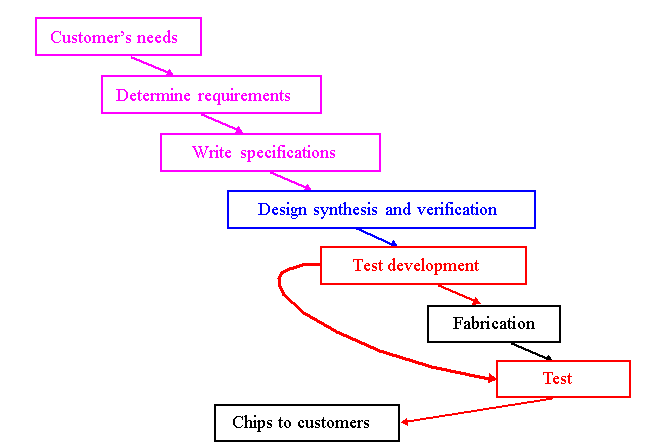
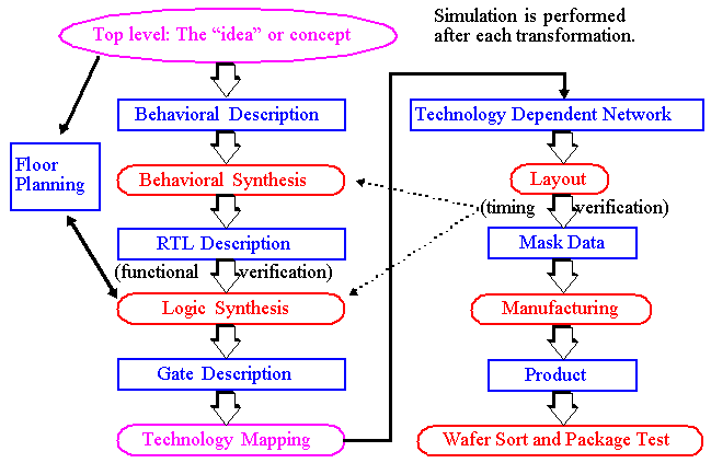
Big Picture
Design Flow Overview
Standard Design Cycle:
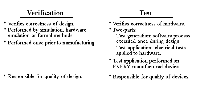
Design Verification vs. Manufacturing Test
Our focus will be on
design verification
and
manufacturing test
of digital integrated circuits.
Verification: Predictive analysis to ensure that the synthesized design, when manufactured, will perform the given I/O function.
Test: A manufacturing step that ensures that the physical device, manufactured from the synthesized design, has no manufacturing defects.
Ideal vs Real Tests
Ideal tests detect all defects produced in a manufacturing process.
Pass all functionally good devices.
Very large numbers and varieties of possible defects need to be tested.
Difficult to generate tests for some real defects (defect-oriented testing is an open problem).
Ideal vs Real Tests
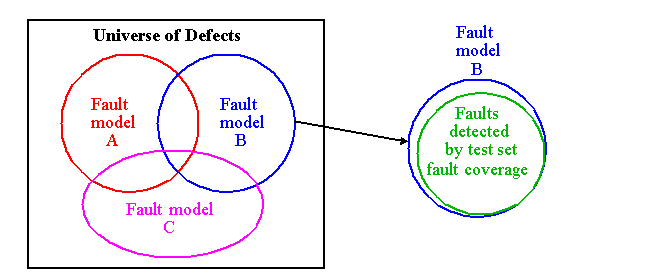
Fault models may not map onto real defects.
A
fault
is a
logic level abstraction
of a
physical defect
that is used to describe the change in the logic function of a device caused by the defect.
It is difficult to generate tests that detect every possible fault in the chip due to high design complexity.
Some good chips are rejected.
The fraction of such chips is called yield loss.
Some bad chips are shipped.
The fraction of bad chips among all passing chips is called defect level (test escapes).
Benefits of Testing:
Quality and economy: Quality means satisfying the user's need at a minimum cost.
VLSI Technology Trends
Year
97-01
03-06
09-12
Feature size (um)
0.25-0.15
0.13-0.10
0.07-0.05
Millions of transistors/cm2
4-10
18-39
84-180
Number of wiring layers
6-7
7-8
8-9
Die size, mm2
50-385
60-520
70-750
Pin count
100-900
160-1475
260-2690
Clock rate, MHz
200-730
530-1100
840-1830
Voltage, V
1.2-2.5
0.9-1.5
0.5-0.9
Power, W
1.2-61
2-96
2.8-109
These trends impact cost and difficulty of testing:
For a yield of 65%, test component of sale price is 27/0.65 = 41.5 cents.
VLSI Technology Trends
EMI (electromagnetic interference)
GHz frequency and inductance cause (1) ringing (2) interference with signal propagation due to dielectric permeability (3) radiation coupling due to sharp rise times.
Increasing Transistor Density:
Feature size reduce by ~%10.5/year leading to density increase of ~%22.1/year.
Wafer and chip size increases in combination with process innovations double this to ~%44/year.
This indicates that # of transistors double every 18 to 24 months (Moore's Law).
Impact on test:
Test complexity increases due to access restrictions.
In the worst case, computational time for test pattern generation increases exponentially with # of PIs and on-chip FFs.
VLSI Technology Trends
For example: Consider a square chip with width = d.
# of transistors, Nt, on the chip is proportional to the area, d2.
# of peripheral I/O pins, Np, is proportional to 4d.
Rent's rule is given by:
Therefore, the test procedure must access a larger number of gates through a proportionately smaller number of pins.
A rough measure of test complexity can be expressed as Nt/Np.
For example, the 97-01 roadmap data indicates 107/900 = 11,000.
Impact on test:
Power dissipation.
VLSI Technology Trends
Constant electric field (CE) scaling keeps the power density constant.
CE scaling not practical in submicron region since switching speed decreases as VDD approaches threshold voltage.
Therefore, supply voltage scaled by
and power density increases by
Testing much check for power grid IR drop and application of the tests must consider power dissipation.
Reducing threshold voltage increases leakage (IDDQ).
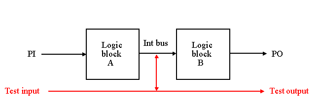
Design for Testability (DFT)
DFT refers to hardware design styles or added hardware that reduces test generation complexity and test application cost.
As indicated above, test generation complexity increases exponentially with size of the chip.
A simple example of simplifying the test generation process:
Roles of Testing
Detection: Go/no-go, is the chip fault-free or faulty.
Must be fast.
Diagnosis: Determine where the failure occurred in the chip and what caused it.
Performed on chips that fail go/no-go tests.
Device characterization: Determination and correction of error in design and/or test procedure.
Failure mode analysis (FMA): Determination of manufacturing process errors that may have caused defects on the chip.