-
Verification testing, characterization testing and design debug:
-
Verifies correctness of design and test procedure.
-
More common to correct design than test procedure.
-
Manufacturing testing:
-
Factory testing of all manufactured chips for parametric faults and for random defects.
-
Acceptance testing (incoming inspection):
-
Customer performs tests on purchased parts to ensure quality.
-
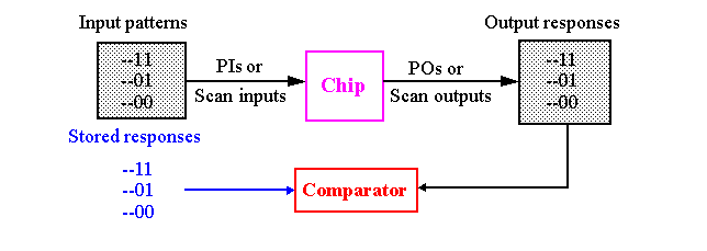
When the chip is digital, the stimuli are called
test patterns
or
test vectors
.
-
Automatic test equipment (ATE) carries out this process.
-
A powerful computer operating under the control of
a
test program, a program written in a high level language
.
-
Digital signal processor (DSP) used for analog testing.
-
Chips are automatically fed to the tester through the wafer handler system.
-
A
probe card
or membrane probe contacts pads of bare or packaged chip.
-
Characterization (design debug or verification testing)
-
Performed on new designs -- determines if design is correct and meets specifications -- very expensive.
-
AC, DC and functional tests performed.
-
Probing of internal chip nodes may also be performed.
-
Specialized tools are used, such as scanning electron microscopes (SEM) and electron beam tests. AI and expect systems may also be useful.
-
Focus on worst case corners -- shmoo plots are created.
-
Characterization
-
The process designed to diagnose and correct errors, sets the final specifications and is used to develop a production test program.
-
Less intensive characterization test performed during normal life-cycle of chip to improve design and process yield.
-
Yield: Fraction of acceptable parts among all fabricated parts.
-
Production (go/no-go test)
-
Less intensive test performed on every chip.
-
Main driver is cost -- test time MUST be minimized.
-
Tests must have high coverage of modeled faults.
-
No fault diagnosis, only an outgoing inspection test.
-
Test at speed of application or speed guaranteed by the supplier.
-
Burn-in (stress test)
-
Some chips that pass production test will fail very quickly thereafter.
-
Burn-in ensures reliability by forcing failure in these "weak" chips.
-
Increasing temperature can accelerate the failure mechanism.
-
Two types of failures are isolated by burn-in:
-
Infant mortality failures: Often caused by a combination of sensitive design and process variation -- short-term burn-in effective (10-30 hours).
-
Freak failures: Same failure mechanism as reliable devices -- long-term burn-in required (100-1000 hours) -- very expensive.
-
Incoming Inspection
-
System manufacturers perform before incorporating chips into systems.
-
Can be similar or more comprehensive than production test.
-
Often done on a random sample of chips.
-
Wafer sort or probe test:
-
Performed before wafer is scribed (cut into chips).
-
Test site characterization is also performed during wafer sort.
-
Test structures are tested to characterize the technology including gate threshold, poly sheet resistance, etc.
-
Sub-types of tests include:
-
Parametric tests.
-
DC parametric tests include shorts test, opens test, leakage test, etc.
-
AC parametric tests include delay test, setup and hold test, etc.
-
Functional Tests.
-
Test every transistor and wire.
-
Designed to cover a high % of modeled faults -- long and expensive.
-
Functional tests (cont.)
-
The test vectors used for verifying that the chip meets specs are called functional vectors.
-
Typically they have low fault coverage (<70%).
-
Functional vectors targeting manufacturing defects usually have higher coverage.
-
We'll distinguish functional patterns in Chapter 4 when we introduce structural test patterns.
-
Functional test may be applied at elevated temperature to guarantee specifications.
-
They can also be used to "speed bin" parts.
-
Accomplished by applying the tests at different voltages and varying the clock frequency.
-
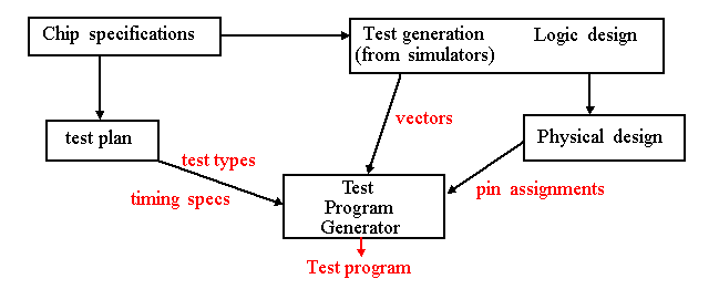
The chip specification document initiates test development.
-
It contains:
-
Functional characteristics, e.g. algorithm to be implemented, I/O signal characteristics (timing and signal levels), clock rate.
-
Type of chip, e.g., microprocessor, memory, mixed-signal, etc.
-
Physical characteristics, e.g., pin assignments, etc.
-
Technology, e.g., gate array, custom, std cell, etc.
-
Environmental characteristics, e.g., operating temperature, supply voltage, etc.
-
Reliability, e.g., acceptance quality level (defects per million, dpm), failure rate per 1,000 hours, noise characteristics.
-
These are used to derive a test plan, which includes
-
Type of test equipment to use, i.e., required clock rate, timing accuracy, etc.
-
Types of tests.
-
Fault coverage requirements.
-
The test program, the digital test vectors and the analog test waveforms are needed once the chip is mounted in the tester.
-
CAD tools to automate the generation of the test programs.
-
3 main purposes of the ATE test data:
-
Accept/reject the chip-under-test (CUT).
-
Provides information about the fabrication process (via FA).
-
Provides information about design weaknesses (via FA).
-
Block diagram for Advantest Model T6682 described in text:
-
Spec for Advantest Model T6682:
-
Chips in the tester itself are 0.35um technology.
-
1024 independently controllable and observable channels.
-
Test speeds are 250MHz, 500MHz and 1GHz.
-
Overall timing accuracy is +/- 200ps.
-
Clock/strobe accuracy is +/- 870ps (80ps for AC measurements).
-
Drive voltages are -2.5 to 6V.
-
Pattern multiplexing (2 patterns written per ATE cycle) used for 500MHz.
-
Pin multiplexing (2 tester channels drive one chip pin) used for 1GHz.
-
SQPG: Sequential pattern generator
-
Stores 16 Mvectors of patterns (vector is # of CUT pins).
-
ALPG: Algorithmic pattern generator
-
32 address bits, 36 data bits.
-
SCPG: Scan pattern generator
-
Supports JTAG, boundary scan
-
Response checking:
-
Pulse train matching: ATE matches bits on 1 channel over 16 cycles or less.
-
Pattern matching mode: ATE matches multiple bits from CUT outputs.
-
Compares with expected output.
-
Result of compare can change the sequence of patterns in real time.
-
Frame processor:
-
Synchronizes the CUT input stimuli (from pattern generators) with sample-and-compare.
-
Strobe time is interval between application of inputs and sampling of outputs.
-
Test head and membrane (cobra) probe card for probing C4s.
-
Pin electronics (PE) of Advantest T6682:
-
Wafer probe: POGO pins interface to Device Interface Board (DIB) and then a probe card.
-
Package test: POGO pins interface with a package handler and then to a testing socket (contactor).
-
ATE has between 128 and 1024 pins, expandable in units of 128.
-
VIH, VIL, VOH, VOL, IH, IL, VT (logic threshold voltage) and both dynamic clam voltages for each channel can be independently set.
-
Parametric measuring unit:
-
Applies and measures voltages or currents at a pin.
-
Two units are available: Multi-DC unit (MDC) and universal DC unit (UDC).
-
Mixed-signal test:
-
ATE has additional components including a waveform generator, a digitizer, digital waveform capture memory, sine wave generator, etc.
-
OS is usually a unix variety, Solaris.
-
Solaris on one processor with non-real time functions.
-
Real-time OS on a second processor for tester control.
-
Test Description Language (TDL) used to write test programs.
-
Can specify strobe times, voltage/current stimuli, vector application rate, vector slew rate, etc.
-
ATE software can:
-
Generate a fail bit map for testing a memory chip.
-
Generate a wafer map showing passing, failing and binning results of chips.
-
Emulate a logic analyzer for debugging.
-
Emulate an oscilloscope for capturing analog waveforms with high resolution.
-
Generate schmoo plots.
-
One ATE can test several (usually identical) devices at the same time.
-
Can be done at wafer probe or package test.
-
Motivation: Most of the cost is for the basic ATE.
-
Adding additional instruments is relatively inexpensive.
-
Digital and mixed signal: Usually can test 2 to 4 chips at time.
-
Memory chips frequently tested 32 and 64 at a time because the test times are very long.

