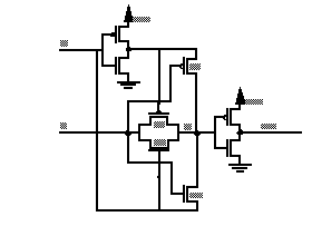
1) a) (6pts) Indicate the transistor(s) that are sources of strong `0's and `1's at node X for each possible combination of values of A and B in the schematic below:
b) (6pts) Indicate the transistor(s) that are sources of weak `0's and `1's at node X for each possible combination of values of A and B in the schematic above.
c) (8pts) Assume the betas for p-channel devices is half the value of n-channel devices. Based on your analysis above, which input transistion sequence, that changes the state of the output, is the fastest ?
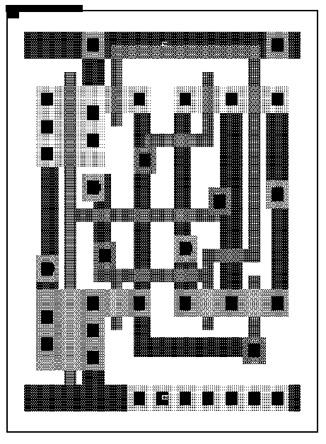
2a) (10pts) Draw a schematic diagram of the magic diagram given on the next page, and presented on the overhead projector. In particular, label the input(s) and output(s) of the circuit.
b) (6pts) Give the truth table for the circuit.
c) (4pts) What function is performed at the output(s) ?

b) (5pts) Draw the minimal CMOS circuit diagram for F = A.B + C + D assuming only A, B, C and D are available.
c) (5pts) Explain how fan-in and fan-out effect the speed of CMOS gate ?
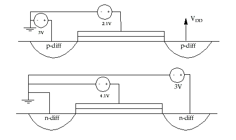
4)a) (6pts) Label each transistor with its region of operation (assume Vt is 1 volt for n-channel transistors and -1 volt for p-channel transistors).
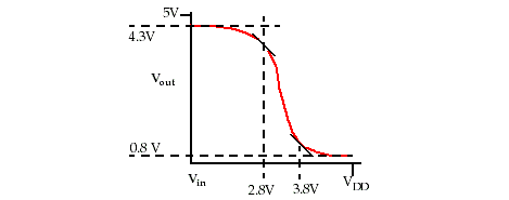
b) (10pts) Compute the low and high noise margins using the following transfer curve.
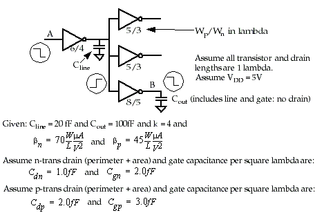
5) a) (3pts) Name the three components of CL at the output of a gate.
b) (17pts) Estimate the delay between nodes A and B for a falling transition on A using the simple gate delay model. CLEARLY INDICATE WHAT YOU ARE CALCULATING !!!!
6)a) (10pts) For the following VHDL code, give a logic diagram (gate level):
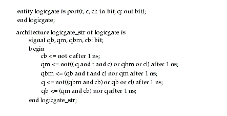
EXTRA CREDIT: For an extra 5 points, tell me what this circuit does and how it works.