1) a) (4 pts) Define self-loading. Is there a benefit to increasing the size of the transistors in gates whose outputs are dominated by self-loading ? Explain in words.
b) (4 pts) What is the primary reason for the reduction in the rise time at the output of the following circuit configurations ? Explain this classic CMOS trade-off (in one sentance).
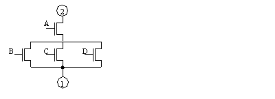
c) (4 pts) Given the n-tree for the function F = (A+B+C).D , which point (1 or 2) would you connect to GND in order to obtain the fastest fall time, if input A was last arriving signal ? Briefly explain in words.
d) (4 pts) Draw the timing diagram for phi1 and phi2 in a 2 phase non-overlapping clock system that illustrates the clock skew problem.
e) (4 pts) Draw the timing diagrams for clk and clk in a single phase global clock system that illustrates each of the two clock skew problems.
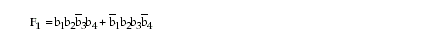
2a) (7 pts) Express the following function in the form required for a NOR PLA.
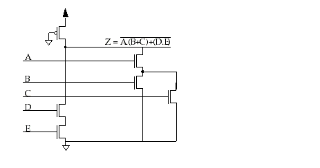
b) (7 pts) Draw a gate level schematic diagram that uses NOR gates and inverters to implement this function.
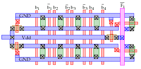
c) (6 pts) Program the following PLA to implement the inverse of F1.
3)a) (4 pts) Name two advantages of pseudo-NMOS over full-complementary CMOS. Name two disadvantages.
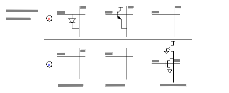
b) (5 pts) Show the modifications required to make a dynamic CMOS gate out of the following pseudo-NMOS gate.
Briefly explain how does dynamic logic address the two disadvantages of pseudo-NMOS ?
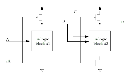
c) (7 pts) Briefly explain the problem associated with cascading dynamic logic (use the following diagram to explain your answer).
3)d) (4 pts) How does domino logic fix this problem ?
4 a) (8 pts) Briefly identify one disadvantage in terms of performance, density and power consumption for each of the following ROMs.
b) (4 pts) With respect to Non-volatile Read-Write memories, there are three types, EPROM, EEPROM, and Flash. What advantage does EEPROM have over UV erasable EPROM ?
c) (4 pts) What advantage does UV eraseable EPROM have over EEPROM ?
d) (4 pts) Why is Flash EEPROM better than UV eraseable EPROM and EEPROM ?
5) a) (6 pts) Draw a transistor level diagram of a six transistor SRAM.
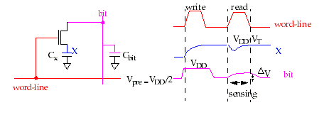
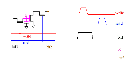
b) (7 pts) Given the 3T DRAM cell shown below, show the electrical behavior of node X and bit2 using the timing diagram for write, read and bit1 shown on the left. Assume that the cell originally stored a 0 and bit2 is precharged to VDD-VT.
Does this cell require refreshing ?
If so, briefly explain one way of accomplishing this ?
Is the operation of reading this cell destructive ?
c) (7 pts) Given the 1T DRAM cell shown below, why is it necessary to use a sense amplifier to read the value of bit ?
Does this cell require refreshing ?
If so, briefly explain one way of accomplishing this ?
Is the operation of reading this cell destructive ?