-
n-type MOS: Majority carriers are electrons.
-
p-type MOS: Majority carriers are holes.
-
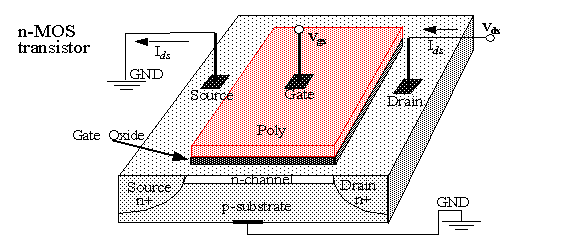
Positive/negative voltage applied to the gate (with respect to substrate) enhances the number of electrons/holes in the channel and increases conductivity between source and drain.
-
V
t
defines the voltage at which a MOS transistor begins to conduct. For voltages less than V
t
(threshold voltage), the channel is cut off.
-
In normal operation, a positive voltage applied between source and drain (V
ds
).
-
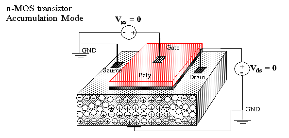
No current flows between source and drain (I
ds
= 0) with V
gs
= 0 because of back to back pn junctions.
-
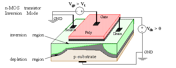
For n-MOS, with V
gs
> V
tn
, electric field attracts electrons creating channel.
-
Channel is p-type silicon which is inverted to n-type by the electrons attracted by the electric field.
-
Three modes based on the magnitude of V
gs
: accumulation, depletion and inversion.
-
With V
ds
non-zero, the channel becomes smaller closer to the drain.
-
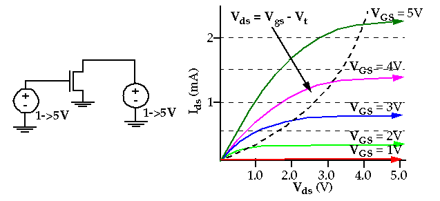
When V
ds
<= V
gs
- V
t
(e.g. V
ds
= 3V, V
gs
= 5V and V
t
= 1V), the channel reaches the drain (since V
gd
> V
t
).
-
This is termed
linear
,
resistive
or
nonsaturated
region. I
ds
is a function of both V
gs
and V
ds
.
-
When V
ds
> V
gs
- V
t
(e.g. V
ds
= 5V, V
gs
= 5V and V
t
= 1V), the channel is
pinched
off close to the drain (since V
gd
< V
t
).
-
This is termed saturated region. I
ds
is a function of V
gs
, almost independent of V
ds
.
-
MOS transistors can be modeled as a voltage controlled switch. I
ds
is an important parameter that determines the behavior, e.g., the speed of the switch.
-
What are the parameters that effect the magnitude of I
ds
? (Assume V
gs
and V
ds
are fixed, e.g. 5V).
-
The distance between source and drain (channel length).
-
The channel width.
-
The threshold voltage.
-
The thickness of the gate oxide layer.
-
The dielectric constant of the gate insulator.
-
The carrier (electron or hole) mobility.
-
Summary of normal conduction characteristics:
-
Cut-off
: accumulation, I
ds
is essentially zero.
-
Nonsaturated
: weak inversion, I
ds
dependent on both V
gs
and V
ds
.
-
Saturated
: strong inversion, I
ds
is ideally independent of V
ds
.
-
V
t
is also an important parameter. What effects its value?
-
Most are related to the material properties. In other words, V
t
is largely determined at the time of fabrication, rather than by circuit conditions, like I
ds
.
-
For example, material parameters that effect V
t
include:
-
The gate conductor material (poly vs. metal).
-
The gate insulation material (SiO
2
).
-
The thickness of the gate material.
-
The channel doping concentration.
-
However, V
t
is also dependent on
-
V
sb
(the voltage between source and substrate), which is normally 0 in digital devices.
-
Temperature: changes by -2mV/degree C for low substrate doping levels.
-
The expression for threshold voltage is given as:
-
Threshold voltage (cont.):
-
Typical values of V
t
for n and p-channel transistors are +/- 700mV.
-
From equations, threshold voltage may be varied by changing:
-
The doping concentration (N
A
).
-
The oxide capacitance (C
ox
).
-
Surface state charge (Q
fc
).
-
As you can see, it is often necessary to adjust V
t
.
-
Two methods are common:
-
Change Q
fc
by introducing a small doped region at the oxide/substrate interface via ion implantation.
-
Change C
ox
by using a different insulating material for the gate.
-
A layer of Si
3
N
4
(silicon nitride) with a relative permittivity of 7.5 is combined with a layer of silicon dioxide (relative permittivity of 3.9).
-
This results in a relative permittivity of about 6.
-
For the same thickness dielectric layer, C
ox
is larger using the combined material, which lowers V
t
.
-
In digital circuits, the substrate is usually held at zero.
-
The sources of n-channel devices, for example, are also held at zero, except in cases of series connections, e.g.,
-
The source-to-substrate (V
sb
) may increase at this connections, e.g. V
sbN1
= 0 but V
sbN2
/= 0.
-
V
sb
adds to the channel-substrate potential:
-
Ideal first order equation for
cut-off
region:
-
Ideal first order equation for
linear
region:
-
Ideal first order equation for
saturation
region:
-
with the following definitions:
-
Process dependent factors:
 .
.
-
Geometry dependent factors: W and L.
-
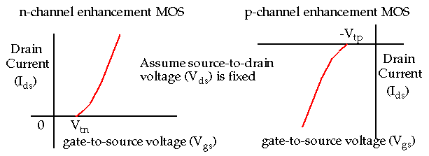
Voltage-current characteristics of the n- and p-transistors.
-
Transistor beta calculation example:
-
Typical values for an n-transistor in 1 micron technology:
-
How does this beta compare with p-devices:
-
n-transistor gains are approximately 2.8 times larger than p-transistors.
-
Inverter DC characteristics
-
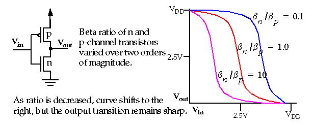
Region C is the most important region. A small change in the input voltage, V
in
, results in a LARGE change in the output voltage, V
out
.
-
This behavior describes an amplifier, the input is amplified at the output. The amplification is termed transistor gain, which is given by beta.
-
Both the n and p-channel transistors have a beta. Varying their ratio will change the characteristics of the output curve.
-
does NOT affect switching performance.
-
What factor would argue for a ratio of 1 for
 ?
?
-
The time required to charge or discharge a capacitive load is equal when
 .
.
-
Since beta is dependent W and L, we can adjust the ratio by changing the sizes of the transistor channel widths, by making p-channel transistors
wider
than n-channel transistors.
-
A parameter that determines the maximum
noise
voltage on the input of a gate that allows the output to remain stable.
-
Two parameters, Low noise margin (NM
L
) and High noise margin (NM
H
).
-
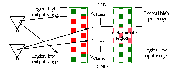
NM
L
= difference in magnitude between the max LOW output voltage of the driving gate and max LOW input voltage recognized by the driven gate.
-
Ideal characteristic: V
IH
= V
IL
= (V
OH
+V
OL
)/2.
-
This implies that the transfer characteristic should switch abruptly (high gain in the transition region).
-
V
IL
found by determining unity gain point from V
OH
.
-
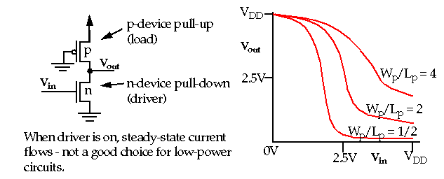
Therefore, the shape of the transfer characteristic and the V
OL
of the inverter is affected by the ratio
 .
.
-
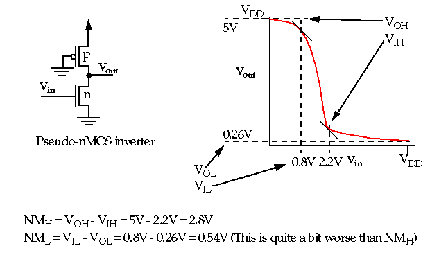
In general, the low noise margin is considerably worse than the high noise margin for Pseudo-nMOS.
-
Pseudo-nMOS was popular for high-speed circuits, static ROMs and PLAs.
-
Example: Calculation of noise margins:
-
The transfer curve for the pseudo-nMOS inverter can be used to calculate the noise margins of identical pseudo-nMOS inverters.




 .
.



 ?
? .
.

 .
.