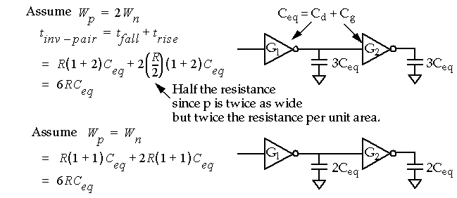
-
So far, we have assumed that to get symmetric rise and fall times:
-
Does this rule reduce overall delay ?
-
Therefore, in
self-loaded
circuits (circuits without significant routing capacitance and fanouts),
equal sized
devices can be used to reduce power dissipation and area without sacrificing performance (overall delay).
-
How do we drive large load capacitances, e.g. off-chip wires via the I/O pads, long buses, etc. ?
-
By using a chain of inverters, where each successive inverter is larger than the previous one.
-
What is the optimal value of
a
(the stage ratio) that both
-
Minimizes the delay through the chain.
-
Minimizes the area and power.
-
The magic number
a
is
e
(~2.7) - see analysis in book.
-
The optimal value may vary depending on process parameters.
-
Two components of power dissipation in CMOS circuits:
-
Static power
-
Dynamic power
-
Static power
dissipation:
-
Reverse-bias leakage current through parasitic diodes formed by source/drain diffusion and n-well diffusion.
-
Through-current of pseudo-nMOS devices.
-
Subthreshold conduction (current that flows when V
in
< V
tn
).
-
Becoming more important as power supply is scaled down.
-
Reverse-bias leakage current
-
Total Static Power dissipation:
-
The current required to charge/discharge capacitive load usually dominates the crowbar (short circuit) current.
-
However, slow rise and fall times will increase crowbar current of driven gates.
-
Assuming a step input and a repetition frequency of f
p
, the average dynamic power, P
d
, is expressed as:
-
Therefore power is proportional to
-
The switching frequency
-
The capacitive load.
-
But goes up as V
DD
2
.
-
Also, power is independent of device parameters, such as V
t
or beta.
-
P
total
= P
s
+ P
d
+ P
short-circuit
(see text P. 236)
-
Detailed analysis of power is often impractical.
-
Consider the following simplifications:
-
Calculate total capacitance driven by the gates in the circuit.
-
Estimate the percentage of the devices operating at the max clock frequency (e.g. 50%).
-
Use the dynamic power dissipation expression:
-
Power minimization:
-
Use complementary logic gates to reduce through current (static)
-
Use minimum-size devices to reduce diffusion leakage (static).
-
Reduce V
DD
, the frequency and the switched capacitance (dynamic).
-
The size of metal conductors is important because:
-
Metal migration.
-
Power supply noise and integrity.
-
RC delay (considered previously).
-
Electro-migration is the transport of metal ions through a conductor induced by direct current.
-
A 'safe' value of current density,
J
, is:
-

-
For example, consider a clock buffer that drives a 100 pF load at 50 MHz:
-
Power supply noise and integrity:
-
IR drops on V
DD
and V
SS
(voltage drops due to current spikes and the resistance of the metal) can occur causing gates to fail.
-
What is the voltage drop (ground bounce) in the power and ground wires if the buffer is 500 microns from the power and ground pads ?
-
Sources of variations that effect nominal circuit behavior (2 environmental, 1 manufacturing):
-
Operating Temperature
-
Supply Voltage: Data sheets give +/- 10%, e.g., 3.0 to 3.6 for 3.3V.
-
Process Variation: Normal to keep parts within 2 or 3 sigma.
-
We must design the circuit to operate over all extremes of these variables.
-
Temperature
:
-
What happens to I
ds
with temperature ?
-
Sources of process variation include changes in doping densities, oxide thickness and line width variations.
-
The following boundary combinations may result
-
Fast-n, Fast-p
-
Fast-n, Slow-p
-
Slow-n, Fast-p
-
Slow-n, Slow-p
-
Yield is influenced by:
-
Technology
-
Chip Area
-
Layout
-
A simple model for yield (Seed's model):
-
Clearly, yield decreases dramatically as the area of the chip increases.
-
Yield and testing are related by
-
Another exponential function that states that if yield is low, we better have high test coverage (+99%) otherwise we ship lots of bad parts.
-
Device testing is a course of its own - stayed tuned.
-
Constant field scaling
: 1/alpha scaling applied to all dimensions, device voltages and concentration densities.
-
I
ds
per transistor scales by 1/alpha.
-
# of transistors per unit area scales by alpha
2
.
-
Current density scales by alpha, power density remains constant (VI/A),
-
e.g., (1/alpha*1/alpha)*alpha
2
-
Constant voltage scaling
: V
DD
is held constant while process is scaled.
-
I
ds
per transistor scales by alpha.
-
# of transistors per unit area scales up by alpha
2
.
-
Current density scales by alpha
3
, power density scales by alpha
3
.
-
Lateral scaling
: Only the gate length is scaled (
gate-shrink
).
-
I
ds
per transistor scales by alpha.
-
# of transistors per unit area scales by alpha.
-
Current density scales by alpha
2
, power density scales by alpha
2
.


