-
The parameters of individual transistors vary from:
-
Lot to lot
(interprocess variation)
-
Wafer to wafer
(interprocess variation)
-
Die to die
(intraprocess variation)
-
The observed random distribution of supposedly identical devices is caused by:
-
Variations in process parameters, e.g.:
-
Impurity concentration densities
-
Oxide thicknesses
-
Diffusion Depths
-
These result from non-uniform conditions during the deposition and/or the diffusion of the impurities (dopants).
-
Changes in these parameters cause electrical parameters to vary, such as sheet resistance and threshold voltage.
-
Causes for observed random distribution (cont):
-
Variations in the dimensions of the devices:
-
Limited resolution of the photolithographic process which causes W/L variations in MOS transistors and mismatches in the emitter areas of bipolar devices.
-
These variations results in dramatic changes in device performance characteristics, in positive and negative directions.
-
This effects the design process, since your design is constrained by a specification, e.g., has to run at 200MHz.
-
In order to account for these variations, you may design your circuit using
worst case
values for all device parameters.
-
While safe, this approach is prohibitively conservative and results in severely
over
designed and hence uneconomical circuits.
-
Moreover, many design parameters are totally uncorrelated.
-
Variations in MOS transistor length is unrelated to variations in t
ox
.
-
An Example:
-
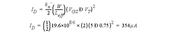
Let's consider a set of different types of variations on an NMOS transistor in a 1.2um CMOS process and the effect they have on its performance.
-
Assume that the device is in saturation with V
GS
= V
DS
= 5V.
-
What is the nominal current of a minimal size device (W = 1.8um, L
eff
= L - 2x
d
= 0.9um):
-
An Example:
-
The following parameters in this expression are subject to variation:
-
V
T
: Which is effected by:
-
Changes in t
ox
.
-
Changes in the dopant levels in the substrate, poly and implants.
-
Surface charge.
-
In the past, threshold voltage could vary by as much as 50%.
-
Today, it is controlled within limits of +/- 25%.
-
k
n
'
: Which is effected by:
-
Changes in oxide thickness is the main contributor to variations in transconductance.
-
Change to mobility (to a lesser degree).
-
An Example:
-
W/L: Which is effected by:
-
The lithographic process.
-
Note that the variations in W and L are uncorrelated, as they are defined in different process steps:
-
W: In the field oxide step.
-
L: In the polysilicon definition and the source and drain diffusion processes.
-
These variations can be assumed to follow a Gaussian distribution.
-
Supply Voltage: Which is effected by:
-
Resistive voltage drops along the supply lines on the PCB.
-
Noise.
-
Let's assume a
25%
variation on V
T
, a
10%
in k
n
'
, a
3
s
change on W and L (0.15um) and a
0.5
V variation in V
DD
(and consequently V
GS
).
-
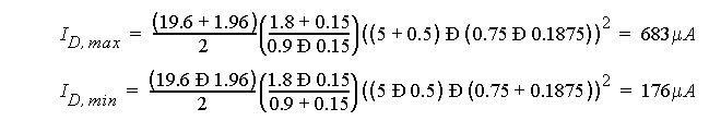
An Example:
-
Putting all of this together for worst- and best-case values for I
D
:
-
This shows the current levels (gain) can vary by as
100%
in the extreme cases.
-
Using the worst-case design approach, it would be necessary to make the transistors
twice
as wide over the nominal case.
-
Ouch (in terms of area)!
-
Fortunately, these worst and best-case conditions are rare.
-
Most designs will display a performance centered around the nominal design.
-
Design for Manufacturability:
-
Objective is to
center the design
so that the majority of the fabricated circuit (99%) fall within the performance specifications, while keeping the area overhead minimal.
-
Tools are available to help with this.
-
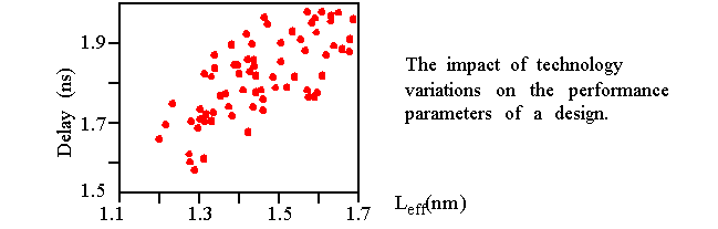
Monte Carlo
analysis involves simulating a circuit over a wide range of randomly chosen device parameters.
-
The result is a distribution plot of design constraints (delay or noise sensitivity) and the simulated variations in these parameters.
-
Therefore SPICE simulations should be taken with a grain of salt.
-
The device parameters used in the model are often
lot-averaged
results.
-
In other words, these parameters are
mean
values and individual device parameters will vary statistically around these values.
-
So, modeling inaccuracies are only one source of variation between actual and simulated device performances.
-
Yet a third source of performance variation is
temperature
.
-
Don't waste your time tweaking picoseconds out of your design using SPICE.