-
These help quantify the quality of a design from different perspectives:
-
Cost.
-
Functionality.
-
Robustness.
-
Performance.
-
Power consumption.
-
Which of these criteria is important is dependent on the
application
:
-
Performance
is important for compute servers.
-
Energy consumption
is a dominant metric for cell-phones.
-
The following analysis focuses on the quality metrics of a simple inverter.
-
These carry forward to the analysis of more complex entities discussed later.
-
Before doing so, let's consider the
cost
of an integrated circuit.
-
Total cost of a product can be broken down into two basic components:
-
Recurring
expenses (
variable cost
).
-
Non-recurring
expenses (
fixed cost
).
-
Fixed cost
is INdependent of sales volume.
-
Effort in time and manpower it takes to produce the design.
-
Indirect costs (company overhead that cannot be billed directly to one product), e.g., R&D, manufacturing equipment, marketing, etc.
-
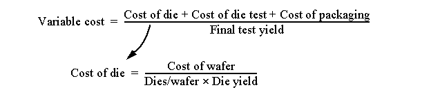
Variable cost
accounts for cost directly attributable to a manufactured product.
-
It is proportional to the product volume and includes:
-
Material cost.
-
Assembly cost.
-
Testing cost.
-
Total cost
:
-
cost/IC = variable cost/IC + (fixed cost/volume).
-
It follows that:
-
The impact of
fixed cost
is more pronounced for
small-volume
products.
-
The design of a microprocessor can afford to support a large design team.
-
The cost to produce a transistor has dropped exponentially over the past decades.
-
However, the form of the equation for
variable cost
has not changed:
-
We will focus on the
cost of the die
in this analysis.
-
It's clear that
Cost of die
is related to chip area.
-
The bigger the die, the more it costs since "Dies/wafer" gets smaller.
-
The actual relation between cost and area is more complex and depends on
die yield
.
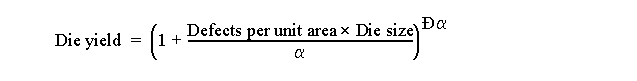
-
Die yield
is related to the number of defects, the size of the die and the complexity of the manufacturing process.
-
Under the assumptions that:
-
Defects are randomly distributed over the wafer.
-
Yield is inversely proportional to the complexity of the fabrication process.
-
Die yield can be expressed as:
-
a is related to the number of masks, a measure of process complexity.
-
It is approximately 3.0 today.
-
Defects per unit area
depends heavily on the maturity of the process but the range 0.5 to 1.0 per cm
2
is typical.
-
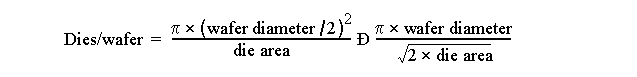
For example, assume:
-
Wafer size is 12 inches.
-
Die size is 2.5 cm
2.
-
1 defects/cm
2.
-
a
is 3.
-
What is the die yield?
-
Dies per wafer
(which takes into account the dies lost along the perimeter):
-
Plugging in yields 252 (=296 - 44) "potentially" operational die.
-
Plugging in for die yield gives
16%!
-
Therefore, on average, only 40 dies will be functional.
-
The bottom line:
-
The number of good dies/wafer = dies/wafer * die yield.
-
The larger and/or more complex the chip, the more costly -- its NOT a
linear
relationship.
-
The designer is going to be interested in using smaller gates, for two reasons:
-
They reduce die size.
-
Smaller gates tend to be
faster
and
consume less energy
.
-
Total gate capacitance (a dominant performance parameter) often scales with area.
-
The
# of transistors
in a gate is often indicative of
implementation area
, although complex interconnect can cause
wiring area
to dominate.
-
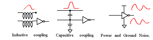
Measured behavior of a manufactured gate normally deviates from the expected response because:
-
Variations in manufacturing process (
process variations
).
-
Dimensions
,
threshold voltage
and
currents
of a MOS transistor can vary significantly between runs, between wafers, and within chips.
-
Noise sources
(unwanted variations of voltages and currents).
-
Unwanted variations of voltages and currents at the logic nodes.
-
Most noise sources are
internal
and proportional to the logic swing.
-
External noise source amplitudes are given in Volts and Amperes.
-
Coping with these is a major challenge in designing for performance.
-
Steady-state parameters of a gate (static behavior) determine how robust it is to manufacturing and noise variations.
-
Their analysis requires an understanding of how digital signals are represented in electronic circuits.
-
The transformation of an
electrical voltage
into a
discrete
variable (logic value abstraction) is accomplished via the definition of nominal voltage levels.
-
V
OH
: High logic level.
-
V
OL
: Low logic level.
-
The difference between
V
OH
and
V
OL
is called the logic or signal swing,
V
sw
.
-
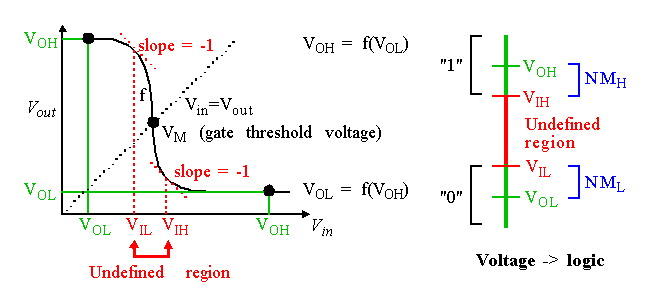
The electrical function of a gate is expressed by its
voltage-transfer characteristic
(
VTC
) or
DC transfer characteristic
.
-
VTC
for an inverter.
-
A graph that plots output voltage as a function of the input voltage,
V
out
= f(
V
in
).
-
Even when an ideal input signal is applied to the input, the output often deviates from the ideal (noise and output loading).
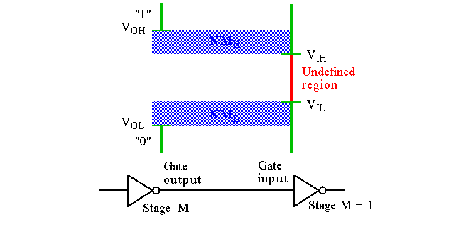
-
Large "1" and "0" intervals are desirable.
-
A measure of the sensitivity of a gate to noise is given by
noise margins
:
-
NM
L
(noise margin low) = V
IL
- V
OL
-
NM
H
(noise margin high) = V
OH
- V
IH
-
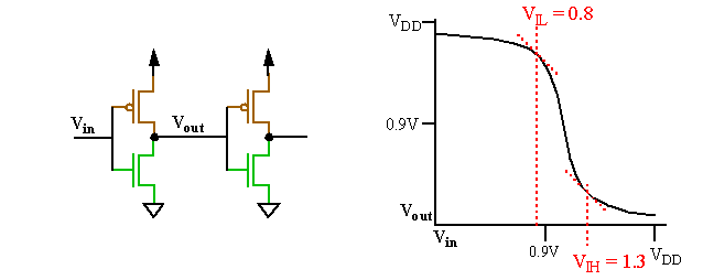
Assume output nominal voltages are:
-
V
OH
= 1.7V
-
V
OL
= 0.1V
-
NM
L
= V
IL
- V
OL
= 0.8 - 0.1 =
700mV
-
NM
H
= V
OH
- V
IH
= 1.8 - 1.3 =
500mV
-
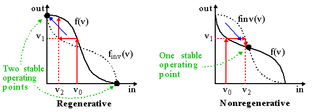
Regenerative Property
:
-
Large noise margins are desirable but
not
a sufficient requirement.
-
The gate must also possess the regenerative property.
-
It's regenerative if the
accumulation
of additional noise sources does NOT drive the signal into the undefined region.
-
Regenerative requires that the
|gain|
be
greater than 1
in the "transient" (undefined) region, bordered by regions with
gains less than 1
.
-
Points
V
IH
and
V
IL
define the borders.
-
Noise immunity
-
Noise margins
expresses the capability of a circuit to "overpower" a noise source.
-
Noise immunity
expresses the ability of a system to process and transmit information correctly in the
presence of noise
.
-
Many circuits that possess low noise margins also have good noise immunity because the
reject a noise source
rather than
overpower it
.
-
Noise sources, as mentioned, are divided into:
-
Sources proportional to the logic swing (V
Np
= g V
sw
).
-
Sources that are fixed (V
Nf
).
-
Noise immunity
-
Assume the noise margin equal
half
the voltage swing.
-
For correct operation, the noise margins have to be
larger
than the sum of the noise values:
-
Therefore, the
minimum signal swing
necessary of system operation is:
-
The signal swing (and noise margin) has to be large enough to overpower the fixed sources.
-
The impact of the internal sources is strongly dependent upon the
noise suppressing capabilities
of the gates, e.g. gj should be small.
-
Directivity:
-
Requires a gate to be
unidirectional
, e.g., changes in an output level should not appear at any unchanging input of the same circuit.
-
Otherwise, noise is generated on gate inputs, affecting
signal integrity
.
-
Full directivity is never achievable in real circuits, primarily because of capacitive coupling.
-
Fan-in and Fan-out:
-
Increasing the fan-out of a gate can affect its logic output levels.
-
From analog amps, ideal is to make
input resistance
of load gates as
large
as possible and the
output resistance
of the driving gate as
small
as possible.
-
Large fan-outs also degrade the
dynamic
performance of the driving gate.
-
Similarly, large fan-ins (# of gate inputs) degrade static and dynamic properties.
-
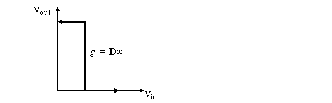
The
Ideal Digital Gate
(from the static perspective):
-
Has
infinite gain
in the transition region.
-
The
gate threshold
is located mid logic swing.
-
High and low noise margins
equal to half the swing.
-
Input/output impedances
are infinity/zero (unlimited fan-out).
-
Impossible but the static CMOS inverter comes close, as we will see.