ECE 321
- Electronics I: Fall 2015
University of New Mexico
Goal:
The goal of this project is to design and
layout a 3-input AOI (AND-OR-Invert) logic cell. AOIs are widely used in
digital and analog electronics. They are key components in CMOS combinational
logic and control path. In this project you are asked to design, layout, and
characterize a basic 3-input AOI logic cell.
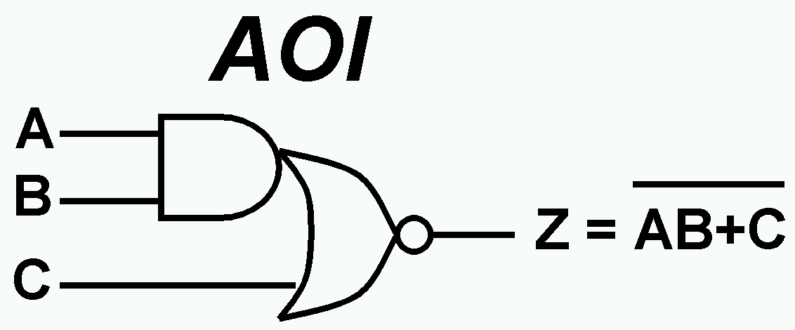
The schematic symbol of the 3-input AOI cell is shown below. In this
project, you will design a 3-input AOI that is optimized for power, delay,
and/or area. Use the layout techniques for cell design that we discussed in
class.
Design
Requirements:
1. The students will form groups of no
more than three for this project. Make sure that the work is divided equally
between the members of each group.
2. There are many ways that you can implement an AOI. Check online resources
and select one type of AOI that you think can provide the best power, area,
or delay tradeoff. Students with minimum delay, minimum power, or minimum
layout area will obtain 10% bonus credit for the project.
3. A
student version of L-Edit is now available for this project. The L-Edit executable
file is ledit.exe for download. All the
design rules and layer definitions are in a setup file ledit.tdb. Ledit reads ledit.tdb, once it is
launched. To perform circuit extraction, the device definition is in template.ext. Copy all three files into
the directory that you create and work for this project. Design your layout,
perform the design rule check (DRC), and extract SPICE file using L-Edit.
To start, you can use this example, ledit_demo.tdb.
Also you can download L-Edit
Quick Start Guide for a brief tutorial for L-Edit.
4. The design rules for this project is a standard 2um process from MOSIS
with 2 metal layers. Download and print the Design Rules for your reference . Use
SCMOS column from the design rule tables.
5. Once the extracted SPICE file is created, use PSPICE transistor model that defines the
MOSFETs and then perform the simulations by adding input voltage sources
and commands to the extracted SPICE file.
6. Use the Power Point Schematic Template
for the schematic drawing for your report.
7.
Use 5V power supply and a 500fF load capacitor in the output for your spice
simulations.
Due Date:
The complete report is due in class on
Wednesday
December 2, 2015
Deliverables:
A written report that contains but not
limited to the following items.
1. Give some brief explanation on how you
designed the AOI cell (for example, schematic, logic style, sizing, etc).
2. Complete layout with X and Y dimensions and the total area.
3. Original SPICE file (circuit netlist).
In your PSPICE file, make sure to include AS, AD, PS, and PD for each transistor
based on your layout.
4. Waveforms from PSPICE simulations that shows the functionality of the
AOI. Clearly show all the data (inputs and outputs) on the waveforms.
5. Using SPICE, measure the worst case switching energy and the worst case
delay of the multiplexer. Use a 500fF load capacitor in your energy and delay
measurement in the PSPICE simulation. Assume the input rise time is very fast
(10ps or less).
6. Summarize your layout area, measured switching energy, and measured
delay in a table.
7. Again using PSPICE, measure the output resistance and the input capacitance
of A, B, and C inputs in your AOI cell. Use a 1pF load capacitor and a 10KOhm
series resistor for your output and input cell characterization.
8. Summarize the cell characterization values (Rout, Cin(A), Cin(B), and
Cin(C)) in a table.
9. A table showing the hour spent for each
task by each member of the group.